AND8242/D
19 V, 3.0 A Universal
Input AC-DC Adaptor
Using NCP1271
Prepared by: Jon Kraft and Kahou Wong
ON Semiconductor
http://onsemi.com
APPLICATION NOTE
INTRODUCTION
This application note presents an example circuit
(Figure 1) using the NCP1271 (65 kHz version) in a flyback
topology. The design steps and subsequent measurements
are also included. An Excel based design worksheet is
available at www.onsemi.com.
The measurements show that the 19 V, 3.0 A circuit
delivers above 85% across a universal input (85 to 265 Vac).
The no load standby consumption is 83 mW at 230 Vac and
the light load operation is greater than 75% efficient.
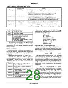
The NCP1271 is one of the latest fixed-frequency
PWM switching controllers with
current-mode
(1) adjustable Soft-Skipt standby operation for low-level
audible noise, (2) integrated high-voltage startup for saving
standby power, (3) timer based overload fault detection, and
(4) internal latch protection features. Table 1 summarizes all
the features of an NCP1271 based power supply.
D1 - D4
Fuse 2A
1N5406 x 4
C5 10 nF
+
19 V / 3 A
-
85 to
265 Vac
T1
E3506-A
D8 MBR3100
D7 MURS160
IC1 NCP1271A
R2 10
R6 10
R7 511
C12
0.15 uF
R8
0.25 / 1W
D10 MZP4746A (18V)
IC4 TL431
Flyback transformer :
Cooper CTX22-17179
Lp = 180uH, leakage 2.5uH max
np : ns : naux = 30 : 6 : 5
C11 1nF/ 1000V
Hi-pot 3600Vac for 1 sec, primary to secondary
Hi-pot 8500Vac for 1 sec, winding to core
Figure 1. Application Circuit Schematic
©ꢀ Semiconductor Components Industries, LLC, 2007
July, 2007 - Rev. 3
1
Publication Order Number:
AND8242/D

 ETC [ ETC ]