AND8318/D
The nominal specified overcurrent trip level in the
voltage plus freewheel diode voltage drop across the
freewheel winding when the MOSFET is off, again by the
relationship dI = (E x dt) /L. Note that L in this case is 1/16
of the full on−state winding inductance because inductance
NCP1014 is 450 mA assuming no tolerance variation. So,
the question here is how can we avoid the above mentioned
low duty cycle issues and possibly get even more output
current from this buck converter using the same
semiconductors with minimal circuit changes.
2
is proportional to N . Since the inductor integrates the
waveform across it, the area under the offtime current
waveform through the freewheel winding is larger than that
of the ontime current waveform, and consequently the
average output current will be higher. The differences seen
by the MOSFET are, of course, the longer ontime (or D’) in
which it conducts current, and a higher turnoff voltage
which will be mentioned below.
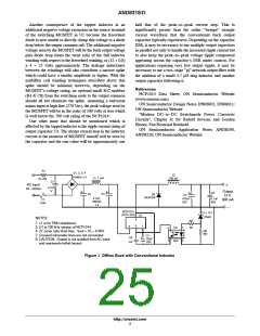
Solution
A modification that will resolve the issues associated with
low duty cycle and even allow a higher output current is
shown in the tapped inductor buck schematic of Figure 2. By
tapping the inductor at 25 percent from the output end and
connecting the freewheeling diode at this node we can
increase the new duty cycle of the MOSFET to
approximately D’ = 0.24 or an on time of 2.4 ms, and the
output current can be increased by about three times, to
almost 1 ampere. The relationships for the extended duty
cycle D’, and the peak current boosting effect, Iboost, are as
follows:
Limitations and Practical Considerations
It is interesting to note that the current boosting benefits
will diminish when the input−to−output voltage differential
is reduced. Taking another look at the current boosting
relationship, Iboost = (N + 1)/[(N x Vout/Vin dc) + 1], shows
that as Vout approaches Vin, the denominator term becomes
N + 1 and the whole expression reduces to unity in the limit
so that no benefit is achieved. At very high input voltages the
value of the expression approaches N + 1 and effective
output current boosting can be achieved by tapping the
inductor at some appropriate point. Note that this
relationship gives the peak current boosting effect and that
the actual output current increase is the weighted average of
the current waveform profile due to the integrating effect of
the inductor. Keep in mind that the freewheel diode will now
have to be current rated to handle this increase in average
output current.
(N)1)
DȀ +
[N)(VVoudct )]
in
where N is the turns ratio of the two windings on either
side of the tap. In this case the winding on the left side or
input side of the tap has three times as many turns as the
winding on the output or freewheel side of the tap. The peak
current boosting capability is given by:
(N ) 1)
Iboost
+
[(N Vout))1]
V
dc
in
The location of the tap on the inductor and how the tap
node is derived is also important due to the detrimental
effects of leakage inductance between the two sections of the
windings. Tapping should be done by using multifilar
winding techniques which allow symmetrical and
interleaved windings that reduce leakage inductance. For
inductor L2 of Figure 2, the coil should be made by flat
winding (no twists) four windings simultaneously
(quadrafilar with four “wires−in−hand”), and then
connecting the four windings in a series aiding manner
(“finish” of one winding to the “start” of the next.) The
connection of the 3 section to the 4 becomes the tap for
the freewheeling diode. This winding technique guarantees
a symmetrical “immersion” of all windings in the magnetic
flux with minimal leakage inductance. For a lower input
voltage the winding configuration could be done bifilar with
just two windings and the tap is at the halfway point where
the windings are connected in series−aiding. In this case N
becomes 1 in the three above equations because the
windings have equal turns. A good rule of thumb is to select
a configuration that places the expanded duty cycle D’
somewhere between 0.2 and 0.5. If D is greater than 0.25
using the conventional buck with D = Vout/Vin relationship,
then a tapped inductor approach will probably not be
beneficial. Practice has shown that tapping the inductor such
that N is either 1, 2, or 3 (depending on the input−to−output
voltage ratio) will usually produce satisfactory results.
The dc voltage input−to−output transfer function now
becomes:
Vindc
Vout
+
(
[
)
N)1 ] * N
D
Why It Works
The statement that current cannot be abruptly
discontinuous in an inductor is actually false as stated. The
fact is, the ampere turns product in an inductor cannot be
discontinuous, i.e., NI must be a constant throughout the
switching period T. In the tapped inductor, the total number
of inductor turns carries the current when the MOSFET is
on, and this current will obviously have to be less than the
specified overcurrent limit in U1. When the MOSFET shuts
off, however, the current in the output side of the winding
must increase abruptly to a peak level four times that of the
on time current to satisfy the ampere turns equality since the
output or freewheel diode winding has one quarter the
number of turns of the entire winding. The current waveform
typical of this transition is shown in Figure 3. Section A is
the magnetizing ramp of the voltage across the entire
inductor when the MOSFET switch is on. When the switch
turns off, a current discontinuity is created at B where the
current rises to a peak level defined by the full winding turns
to freewheel diode winding turns ratio (4:1). The current
ramp−down slope of C is defined by the value of the output
rd
th
http://onsemi.com
2

 ETC [ ETC ]