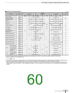
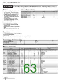
SI-8511NVS
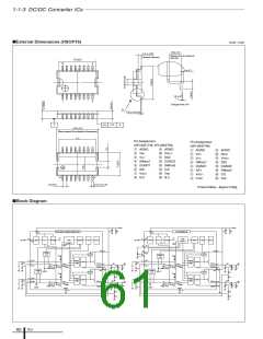
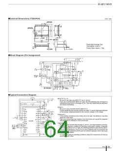
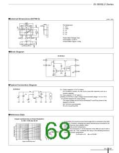
■External Dimensions (TSSOP24)
(Unit : mm)
2.0
φ
Mirror surface
Depth 0.02 to 0.08
A
°
11
24
13
°
11
1.0
φ
Mirror surface
Depth 0.02 to 0.08
3.00
°
11
1
12
°
11
0.65
0.375 TYP
+0.1
0.22
–0.05
0.12
M
A
7.80±0.1
7.9±0.2
0.4
Plastic Mold Package Type
Flammability: UL94V-0
S
Product Mass: Approx. 1.36g
0.50±0.2
0.08
S
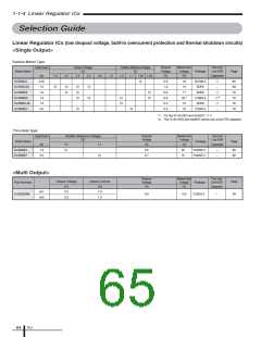
■Block Diagram (Pin Assignment)
VIN
+
+5V
V
CC
1
ILIM
V
IN ISEN
VCC2
OCP
PRE_REG
Vpreg
VH
EN
Level
Shift
EN
Latch
Buff
H : ON
: OFF
UVLO
Gate Driver
OFF Clamp
DRVH
LIN
L
VO
Synchronous
Cont.
(Logic)
+
Logic
Buff
POWER_GOOD
H : GOOD
Power
Good
DRVL
PGND
PWRGD
L
: NG
–
+
Switching
VO
Constant On
Time Cont.
VSNS
+
COMP
–
–
+
OSC
SS
GND
OVP_SL
14
12
FADJ
FSET
SS
SKIP
Open : Change Frequency
Short : 400KHz Operation
Open : Skip Mode
: No Skip Mode
L
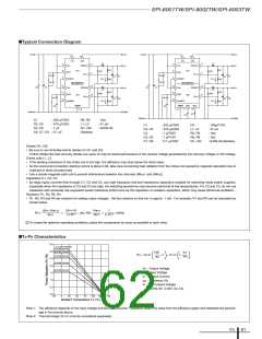
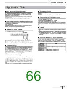
■Typical Connection Diagram
MOS FET Q1, Q2
• Be sure to use logic type MOS FET as Q1 and Q2.
V
IN
R2
µ
C1 : 10
F
V
CC : 5V
If you use a normal power MOS FET type, the ON resistance may not drop to a
satisfactory level due to a shortage of VGS. This may deteriorate the efficiency
and cause overheating.
µ
C7 : 0.1 F
D2 : SFPL52
R1
5mΩ
R5
10Ω
Diode D1
Q1
• Be sure to use a Schottky-barrier diode for D1.
If other diodes like fast recovery diodes are used, IC may be destroyed because
of the reverse voltage generated by the recovery voltage or ON voltage.
1
24
NC
NC
LIN
µ
L1 : 10
H
2
23
22
21
20
19
18
17
16
15
14
13
DRVH
V
O
+
Q2
3
C2 :
VH
DRVL
PGND
D1
µ
330
F
R6
10Ω
Choke coil L1
SJPJ-L3
4
V
IN
• If the winding resistance of the choke coil is too high, the efficiency may drop
below the rated value.
• Take care concerning heat radiation from the choke coil caused by magnetic
saturation due to overload or short-circuit load.
C9
1000
pF
C6
0.1 ~ 1
5
6
R13
µ
C5 : 4.7
F
ISEN
ILIN
VCC2
µ
F
OVP_SL
R12
F
SI-8511NVS
7
µ
C4 : 3.3
C8 : 220pF
GND
VSNS
VCC1
V
CC
Capacitor C1, C2
8
SS
EN
R4
47kΩ
EN
• As large ripple currents flow through C1 and C2, use high-frequency and low-
impedance capacitors suitable for switching mode power supplies. Especially
when the impedance of C2 is high, the switching waveform may become abnor-
mal at low temperatures. For C2, do not use a capacitor with an extremely low
equivalent series resistance (ESR) such as a ceramic capacitor, which may cause
an abnormal oscillation.
V
R7
47kΩ
CC
R9
R10
2.2kΩ
9
V
O
C3
0.1
SKIP
10
11
12
µ
F
PWRGD
REF
SKIP
FADJ
NC
PWRGD
NC
R11 : 100kΩ
* To create the optimum operating conditions, place the components as close as
possible to each other.
R8 : 200kΩ
ICs
63

 ETC [ ETC ]