SI-3000LU Series
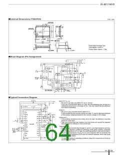
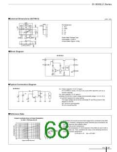
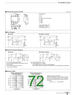
■External Dimensions (SOT89-5)
(Unit : mm)
4.5±0.05
1.6±0.05
0.4±0.03
Pin Assignment
q ADJ
w GND
e VC
4.2±0.05
t
4.2±0.05
4.2±0.05
r
0.1±0.05
φ
r VIN
t VO
4.7±0.05
4.2±0.05
4.2±0.05
Plastic Mold Package Type
Flammability: UL94V-0
q
w
e
Product Mass: Approx. 0.05g
1.5±0.05
1.5±0.05
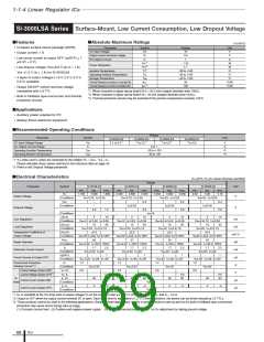
■Block Diagram
SI-3012LU
V
IN
VO
4
3
5
1
V
C
ADJ
TSD
+
–
2
GND
REF
■Typical Connection Diagram
SI-3012LU
CO: Output capacitor (10 µF or larger)
VIN
VO
For SI-3000LU series, Co has to be a low ESR capacitor such as a
ceramic capacitor.
4
3
5
1
R
1
2
CIN
+
CIN: Input capacitor (10 µF approx.)
A
DJ
Setting of SI-3012LU output voltage (recommended voltage: 1.5 V to 15 V)
2
•
VIN
R
GND
R1 and R2: Resistors for output setting
The output voltage can be set by connecting R1 and R2 as shown in the
diagram on the left.
VC
R2: 100 kΩ is recommended
R1=(VO–VADJ)/(VADJ/R2)
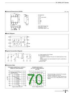
■Reference Data
Copper Laminate Area vs Power Dissipation
Tj=100°C PCB size 40×40
• A monolithic ICs mounts an inner frame stage that is connected to the GND
pin (pin 2). Therefore, enlarging the copper laminate area connected to the
GND pin improves heat radiation effect.
1
Ta=25°C
0.9
Ta=40°C
Ta=60°C
0.8
• Obtaining the junction temperature
Ta=85°C
0.7
Measure the temperature TC at the lead part of the GND pin (pin 2) with a
thermocouple, etc. Then, substitute this value in the following formula to
obtain the junction temperature.
0.6
0.5
0.4
0.3
0.2
0.1
0
Case temperature Tc
measurement point
Tj=PD×θj–c+Tc (θj–c=5°C/W)
10
100
1000
Copper Laminate Area (mm2)
ICs
67

 ETC [ ETC ]