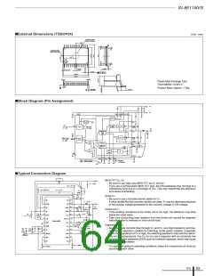
1-1-3 DC/DC Converter ICs
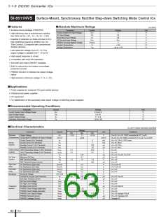
SI-8511NVS Surface-Mount, Synchronous Rectifier Step-down Switching Mode Control ICs
■Features
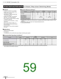
■Absolute Maximum Ratings
(Ta=25°C)
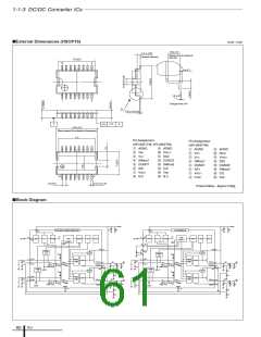
• Surface-mount package (TSSOP24)
Parameter
Control-System DC Input Voltage
DC Input Voltage
Symbol
Ratings
Unit
V
VCC
7
• High efficiency due to synchronous rectifica-
tion: 92% (at VIN = 5V, IO = 1A, VO = 2.5V)
VIN
25
V
Boost Block Input Voltage
EN Terminal Input Voltage
PWRGD Terminal Applied Voltage
Junction Temperature
VH
30
VCC
V
• Capable of downsize a choke-coil due to IC's
high switching frequency (400kHz typ, On
Time Control). (Compared with conventional
Sanken devices)
VEN
V
VPWRGD
Tj
7
V
+150
°C
°C
Storage Temperature
Tstg
–40 to +150
• Low reference voltage (Vref) of 1.1V. The
output voltage is variable from 1.1V to 6V.
• High-speed response to a load
• Compatible with low ESR capacitors
• Soft start and output ON/OFF available
• Built-in overcurrent and output-overvoltage
protection circuits
• PWRGD function to indicate the output voltage
status
• High precision reference voltage: 1.1V ± 1.2%
■Applications
• Power supplies for notebook PCs and mobile devices
• Onboard local power supplies
• OA equipment
• For stabilization of the secondary-side output voltage of switching power supplies
■Recommended Operating Conditions
Parameter
Control System Input Voltage Range
Input Voltage Range
Symbol
VCC
VIN
Ratings
Unit
V
4.5 to 5.5
3 to 18
V
Output Voltage Range
VO
1.1 to 6
V
Operating Temperature Range
Top
–20 to +85
°C
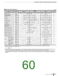
■Electrical Characteristics
(Ta=25°C unless otherwise specified)
Ratings
typ.
Parameter
Symbol
Unit
Conditions
min.
max.
Dynamic
Characteristics
Output Voltage
VO
∆VO/∆T
Iop
–1.2%
1.1
+1.2%
V
mV/°C
mA
mA
µA
µA
V
VIN=5V, VCC=5V, VSNS connected to VO, IO=0A
IN=5V, VCC=5V, VSNS connected to VO, I =0A, T =0 to 85°C
Temperature Coefficient of Output Voltage
Circuit Current (VCC Terminal)
Circuit Current (VIN Terminal)
Standby Current 1 (VCC Terminal)
Standby Current 2 (VIN Terminal)
±0.03
V
O
a
6
1
VCC=5V, EN=H, FADJ:open
VIN=5V, EN=H
VCC=5V, EN=L
VIN=5V, EN=L
VIN=5V
Circuit
Current
Iop
Istd1
100
50
Istd2
Undervoltage UVLO Operating Voltage 1 (VCC Terminal)
Lockout
Vuvlo1
Vuvlo2
Ton
3.7
2.5
4.45
2.9
UVLO Operating Voltage 2 (VIN Terminal)
On Time
V
VCC=5V
1.27
0.7
µS
µS
V
VCC=5V, VIN=5V, VO=2.5V
VCC=5V
On Time
Control
Minimum Off Time
Toff
REF Terminal Voltage
Vref
1.1
1.2
1.3
VCC=5V
REF Terminal Source Current
On Resistance (high side)
On Resistance (low side)
On Resistance (high side)
On Resistance (low side)
Bootstrap Voltage
Iref
100
µA
Ω
VCC=5V
High Side
Drive
RonHH
RonHL
RonLH
RonLL
VH-VLIN
Ilim
5.5
5.5
5.5
5.5
5
VH-VLIN=5V
VH-VLIN=5V
VCC=5V
Ω
Low Side
Drive
Ω
Ω
VCC=5V
Bootstrap
4.5
90
5.5
V
Current for Current Limit Detection
Soft Start Terminal Current
EN Low Level Voltage
100
±20
110
µA
µA
V
VCC=5V, VIN=5V
VCC=5V
Iss
Vcelo
Vcehi
ICE
0
0.8
VCC
5
VCC=5V
EN High Level Voltage
2.4
V
VCC=5V
Protection
System
EN Bias Level Current
µA
V
VCC=5V, EN=5V
VCC=5V
PWRGD Good Voltage (high side)
PWRGD Good Voltage (low side)
PWRGD Low Output Voltage
PWRGD Terminal Current
PWRGD Leakage Current
Vsens
Vsens
Vpwrgd
Ipwrgd
Ipwrgd
1.32
0.88
V
VCC=5V
0.4
120
5
V
VCC=5V, Ipwrgd=120µA
VCC=5V, Vpwrgd=0.4V
Vpwrgd=5V
µA
µA
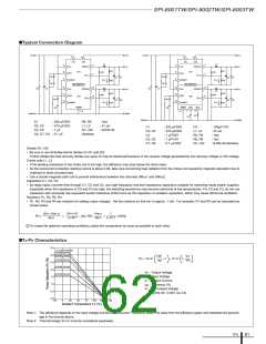
ICs
62

 ETC [ ETC ]