1-1-4 Linear Regulator ICs
SI-3000LU Series Surface-Mount, Low Current Consumption, Low Dropout Voltage
■Features
■Absolute Maximum Ratings
(Ta=25°C)
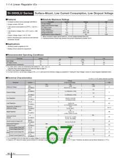
• Compact surface-mount package (SOT89-5)
Parameter
Symbol
Ratings
18
Unit
V
DC Input Voltage
VIN
• Output current: 250 mA
Output control terminal voltage
DC Output Current
VC
VIN
V
• Low current consumption lq (OFF) ≤ 1µA (VC =
IO
250
mA
W
0 V)
*1
Power Dissipation
PD
0.75
*2
Junction Temperature
Tj
–40 to +135
–40 to +125
146
°C
• Low dropout voltage: VDIF ≤ 0.5 V (at IO = 250
*2
Storage Temperature
Tstg
°C
mA)
*1
Thermal Resistance (Junction to Ambient Air)
θ j-a
°C/W
• Output voltage range (1.5V to 15V)
*1: When mounted on glass-epoxy board 40 × 40 mm (copper laminate area 2%).
*2: Thermal protection circuits may operate if the junction temperature exceeds 135°C.
• Built-in drooping-type-overcurrent and thermal
protection circuits
■Applications
• Auxiliary power supplies for PC
• Battery-driven electronic equipment
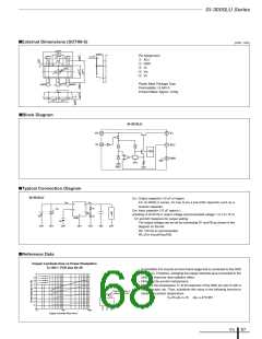
■Recommended Operating Conditions
Ratings
Parameter
Symbol
Unit
min.
*2, *3
max.
VO+2*1
250
Input Voltage
VIN
IO
V
DC Output Current
0
mA
°C
Operating Ambient Temperature
Top
–20
85
*1: VIN (max) and IO (max) are restricted by the relation PD = (VIN - VO) × IO.
Calculate these values referring to the reference data on page 67.
*2: Refer to the Dropout Voltage parameter.
*3: For the SI-3012LU, set the input voltage to Vin ≥ 2.4 V, and secure the minimum voltage as explained in "Setting DC Input Voltage" section in Linear Regulator Application Note.
■Electrical Characteristics
(Ta=25°C, VC=2V, unless otherwise specified)
Ratings
Parameter
Symbol
SI-3012LU(Variable)
Unit
V
min.
typ.
max.
VADJ
1.210
1.250
1.290
Reference Voltage
Conditions
VIN=VO+1V, IO =10mA
V
DIF
0.3
0.5
10
Conditions
I
I
O
O
=100mA(V
O
=3.3V)
=3.3V)
Dropout Voltage
V
Conditions
=250mA(V
O
∆VLINE
Line Regulation
Load Regulation
V
IN=V
=10mA( VO
O
+1 to V
O
+5V,
mV
mV
Conditions
∆VLOAD
I
O
=3.3V)
20
V
IN=VO +1V,
Conditions
IO
=1 to 250mA( V
O=3.3V)
Temperature Coefficient of
Reference Voltage
∆V
O/∆Ta
0.3
mV/°C
Tj=0 to 100°C
Conditions
RREJ
55
Ripple Rejection
dB
V
IN=V
O
+1V,
O
Conditions
f=100 to 120H
Z( V =3.3V)
I
q
150
1
Quiescent Circuit
Current
µA
V
V
IN=V
O+1V, IO=0mA
Conditions
C=2V, R2=100kΩ
I
q
(OFF)
Circuit Current at Output OFF
µA
mA
V
Conditions
V
IN=VO+1V,VC=0V
Overcurrent Protection
Starting Current*1
I
S1
260
2.0
Conditions
, IH
VIN=VO +1V
Control Voltage (Output ON)*2
Control Voltage (Output OFF)*2
VC
V
C
, IL
0.8
40
V
C
I
C
, IH
Control Current (Output ON)
Control Current (Output OFF)
µA
µA
Terminal
Conditions
, IL
Conditions
VC=2V
0
I
C
–5
V
C=0V
*1: Is1 is specified at the 5% drop point of output voltage VO on the condition that VIN = 3.3 V, and IO = 10 mA.
*2: Output is OFF when the output control terminal (VC terminal) is open. Each input level is equivalent to LS-TTL level. Therefore, the device can be driven directly by LS-TTLs.
ICs
66

 ETC [ ETC ]