SPI-8001TW/SPI-8002TW/SPI-8003TW
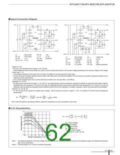
■Typical Connection Diagram
V
IN
V
C/E
V
IN
V
C/F
3
14
C/E
SWout1
3
15
C/E
SWout1
V
CC
VCC
L1
L1
2
6
5
4
7
2
6
5
4
7
V
IN1
VIN1
V
01
V
C1
R1
R2
R1
R2
Ch1
Ch1
Di1
Di1
SS1
SS1
+
+
V
REF1
VREF1
R5
C4
R5
C5
C2 C7
C2 C7
I
REF1
I
REF1
DGND1
SPI-8000TW
SWout2
DGND1
SPI-8003TW
VIN2 SWout2
+
+
15
11
12
13
10
16
12
13
14
11
C6
C1
C4
C1
V
IN2
V
02
V
C2
L2
L2
R3
R4
R3
R4
Di2
Di2
SS2
SS2
Ch2
Ch2
+
+
V
REF2
VREF2
R6
C5
R6
C6
C3 C8
C3 C8
I
REF2
IREF2
DGND2
DGND2
AGND
AGND
C
ORC
RCSC
8
1, 9
1, 9
10
R7
GND
GND
C9
GND
GND
C1
: 220 µF/50V
: 470 µF/25V
: 1 µF
R5, R6
L1, L2
: 1kΩ
C2, C3
C4, C5
: 47 µH
C1
: 220 µF/50V
: 470 µF/25V
: 1 µF/50V
C9
: 100pF/10V
: 47 µH
: 1kΩ
Di1, Di2
: SJPB-H6
C2, C3
C4
L1, L2
R2, R4
R5, R6
C6, C7, C8 : 0.1 µF
(Sanken)
C5, C6
C7, C8
: 1 µF/10V
: 1kΩ
: 0.1 µF/50V
Di1, Di2
: SJPB-H6 (Sanken)
Diodes Di1, Di2
• Be sure to use Schottky-barrier diodes for Di1 and Di2.
If other diodes like fast recovery diodes are used, IC may be destroyed because of the reverse voltage generated by the recovery voltage or ON voltage.
Choke coils L1, L2
•
•
If the winding resistance of the choke coil is too high, the efficiency may drop below the rated value.
As the overcurrent protection starting current is about 2.0A, take care concerning heat radiation from the choke coil caused by magnetic saturation due to
overload or short-circuited load.
•
Use a closed-magnetic-path coil to prevent interference between the channels SWout1 and SWout2.
Capacitors C1, C2, C3
•
As large ripple currents flow through C1, C2 and C3, use high-frequency and low-impedance capacitors suitable for switching mode power supplies.
Especially when the impedance of C2 and C3 are high, the switching waveforms may become abnormal at low temperatures. For C2 and C3, do not use
capacitors with extremely low equivalent series resistance (ESR) such as OS capacitors or tantalum capacitors, which may cause abnormal oscillation.
Resistors R1, R2, R3, R4
•
R1, R2, R3 and R4 are resistors for setting output voltages. Set the resistors so that IREF is approx. 1 mA. For example, R1 and R2 can be calculated as
shown below.
(VO1–VREF1)
IREF1
(VO1–V)
1×10⁻³
VREF1
IREF1
1
.
=
1(KΩ)
.
R1=
=
(Ω), R2=
=
1×10⁻³
To create the optimum operating conditions, place the components as close as possible to each other.
■Ta-PD Characteristics
3.5
θ
j-a (Copper Laminate Area)
35.8°C/W (30.8 cm2
)
)
38.2°C/W (15.6 cm2
3.0
2.5
2.0
1.5
1.0
0.5
0.0
100
VO
PD = VO·IO
–1 – VF·IO 1–
42.6°C/W (8.64 cm2
)
ηχ
VIN
52.3°C/W (3.34 cm2
69.2°C/W (0.84 cm2
)
VO : Output Voltage
VIN : Input Voltage
)
IO : Output Current
ηχ : Efficiency (%)
VF : D1 Forward Voltage
SJPB-H6···0.45V (IO=1A)
–25
0
25
50
75
100 125 135 150
Ambient Temperature Ta (°C)
Note 1: The efficiency depends on the input voltage and the output current. Therefore, obtain the value from the efficiency graph and substitute the percent-
age in the formula above.
Note 2: Thermal design for D1 must be considered separately.
ICs
61

 ETC [ ETC ]