SI-7321M
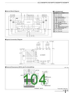
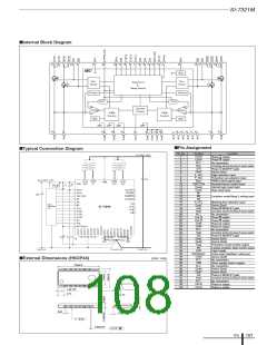
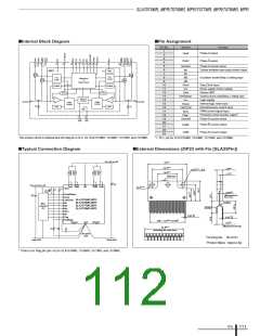
■Internal Block Diagram
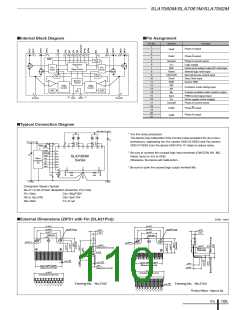
■Pin Assignment
■Typical Connection Diagram
Pin No.
1
Symbol
Out/A
Out/A
N.C.
Function
Phase A output
Phase A output
2
3
No connection
4
5
6
7
8
9
RsA
G/A
Connection terminal for phase A sense resistor
Phase A MOSFET gate
Device Gnd1
Gnd1
E_SEL
P_SEL
Sync
CW/CCW
Reset
Clock
M1
M2
M3
B_SEL
Gnd1
G/B
Edge selection input
Protection use selection input
PWM control signal input
Normal/reverse control input
Internal logic reset input
Step clock input
10
11
12
13
14
15
16
17
18
19
20
21
22
23
24
25
26
27
28
29
30
31
32
33
34
35
36
37
38
39
40
41
42
43
44
Excitation mode/Sleep 2 setting input
Blanking time selection input
Device Gnd1
Phase B MOSFET gate
Connection terminal for phase B sense resistor
No connection
Phase B output
Phase B output
Phase B output
Phase B output
RsB
N.C.
Out /B
Out /B
OutB
OutB
N.C.
RsB
GB
Gnd1
Gnd2
Flag
Mo
VDD
Ref/Sleep1
Gnd3
N.C.
VBB
N.C.
Gnd4
Gnd1
GA
No connection
Connection terminal for phase B sense resistor
Phase B MOSFET gate
Device Gnd1
Device Gnd2
Protection circuit monitor output
2-phase excitation state monitor output
Logic supply
Control current mode/Sleep 1 setting input
Device Gnd3
No connection
Driver supply (motor supply)
No connection
Device Gnd4
■External Dimensions (HSOP44)
(Unit : mm)
18.6±0.3
Device Gnd1
Phase A MOSFET gate
Connection terminal for phase A sense resistor
No connection
Phase A output
Phase A output
RsA
N.C.
Out A
Out A
1.50 TYP
2.17
0 to 10°
0.65
0.5±0.2
0.10
0.22±0.05
M
0.12
ICs
107

 ETC [ ETC ]