1-2-1 2-Phase Stepper Motor Unipolar Driver ICs
SI-7321M 2-Phase to 4W 1-2 Phase Excitation Support, Built-in Sequencer
■Features
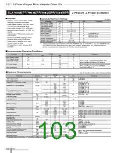
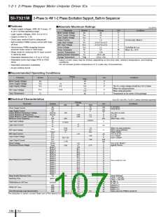
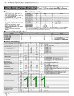
■Absolute Maximum Ratings
(Ta=25°C)
• Power supply voltages, VBB: 46 V (max), 10
to 44 V normal operating range
Parameter
Motor Supply Voltage
Driver Supply Voltage
Logic Supply Voltage
Output Current
Symbol
VM
Ratings
Unit
V
V
V
A
Conditions
46
• Logic supply voltages, VDD: 3.0 to 5.5 V
• Output Current Io: 1.5A
VBB
VDD
Io
46
6
1.5
• Clock input method (built-in sequencer)
Current ratio: Mode F
• Self-excitation PWM current control with fixed
off time
Logic Input Voltage
REF Input Voltage
Sense Voltage
VIN
–0.3 to VDD+0.3
–0.3 to VDD+0.3
±2
V
V
V
W
℃
℃
℃
VREF
VRS
PD
• Synchronous PWM chopping function
prevents motor noise in Hold mode
Excluding tw<1µs
When Ta = 25°C
Power Dissipation
Junction Temperature
Operating Ambient Temperature
Storage Temperature
3.5
• Sleep mode for reducing the IC input current
in stand-by state
Tj
Ta
Tstg
+150
–20 to +80
–30 to +150
• Selectable blanking time (1.8 us or 3.6 us)
• Selectable clock input edge (POS or POS/
NEG)
*: Output current value may be limited, depending on the duty ratio, ambient temperature, and heating
conditions.
Do not exceed junction temperature of Tj under any circumstances.
• Selectable protection availability
• 44-pin surface-mount
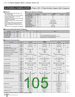
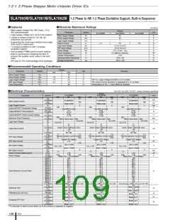
■Recommended Operating Conditions
Ratings
Parameter
Symbol
Unit
Conditions
min.
max.
44
44
5.5
1.0
0.5
85
Motor Supply Voltage
Driver Supply Voltage
Logic Supply Voltage
VM
VBB
VDD
V
V
V
10
3.3
The VDD surge voltage should be 0.5V or lower.
When not using protection
VREF
Tc
0.04
V
REF Input Voltage
Case Temperature
When using protection
℃
Temperature at the center of the package
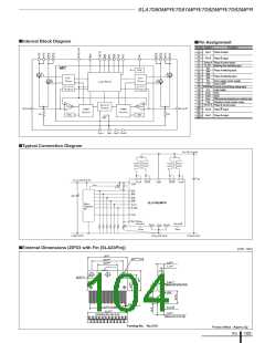
■Electrical Characteristics
(VDD=5V, VBB=24V, Ta=25°C, unless otherwise specified)
Ratings
typ.
Parameter
Symbol
Unit
Conditions
min.
100
max.
15
100
IBB
IBBS
IDD
V(BR)DSS
RDS(ON)
VF
mA
µA
mA
V
Ω
V
In operation
Sleep Mode
Driver Supply Current
Logic Supply Current
5
Output MOSFET Breakdown Voltage
Output MOSFET ON Resistance
Output MOSFET Diode Forward Voltage
Maximum Clock Frequency
VBB=44V, ID=1mA
ID=1.5A
IF=1.5A
0.25
0.95
0.4
1.2
Fclk
250
kHz
When Duty = 50%
VIL
VIH
0.25VDD
Logic Input Voltage
V
0.75VDD
IIL
IIH
±1
±1
Logic Input Current
µA
0.04
0.04
2
1.5
0.6
VDD
When not using protection
When using protection
Sleep1 Mode
VREF=0 to VDD
ILOL=1.25mA
VREF
REF Input Voltage
V
VREFS
IREF
VLOL
VLOH
ILOL
ILOH
VSENSE
Vocp
REF Input Current
±10
µA
V
V
mA
mA
V
1.25
1.25
Logic Output Voltage
VDD-1.25
–1.25
ILOH=–1.25mA
Logic Output Current
Sense Voltage
Overcurrent Sense Voltage
0.2
0.7
VREF=0.2V, Mode F
against Vsence
0.65
0.75
V
Mode F
Mode E
Mode D
Mode C
Mode B
Mode A
Mode 9
Mode 8
Mode 7
Mode 6
Mode 5
Mode 4
Mode 3
Mode 2
Mode 1
TSE
100
%
%
%
%
%
%
%
%
%
%
%
%
%
%
%
µS
µS
µS
µs
µs
µs
µs
µs
µs
98.1
95.7
92.4
88.2
83.1
77.3
70.7
63.4
55.5
47.1
38.2
29.0
19.5
9.8
Step Reference Current Ratio
VREF=0.04V to 1.5V
Sleep-Enable Recovery Time
Switching Time
100
1.5
Sleep1&Sleep2
Clock → Out ON
Clock → Out OFF
B_SEL: L
B_SEL: H
Mode8 to F
Mode4 to 7
Mode1 to 3
Starts when the PWM is turned off.
2.0
1.5
1.8
3.6
13
9.5
7.5
2
tpdon1
PWM Minimum ON Time
ton(min)
toff1
toff2
toff3
topp
PWM OFF Time
Time Not Sensing Load Disconnection
2.5
The direction in which current flows out of the device is regarded as negative.
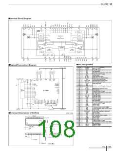
ICs
106

 ETC [ ETC ]