ICL8052A/ICL71C03, ICL8068A/ICL71C03
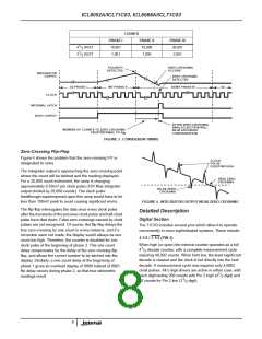
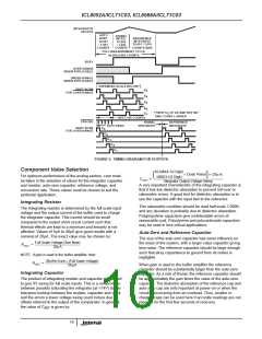
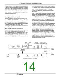
INTEGRATOR
OUTPUT
AUTO
ZERO
10,001
/ 1,001
COUNTS
SIGNAL
INTEG.
10,000
REFERENCE
INTEGRATE
20,001 / 2,001
/ 1,000
COUNTS
COUNTS MAX
FULL MEASUREMENT CYCLE
40,002/4,002 COUNTS
BUSY
OVER-RANGE
WHEN APPLICABLE
UNDER-RANGE
WHEN APPLICABLE
EXPANDED SCALE BELOW
DIGIT SCAN
D
5
4
3
FOR OVER-RANGE
D
D
D
D
2
1
†FIRST D OF AZ AND REF INT
5
ONE COUNT LONGER
1000†/100 COUNTS
STROBE
SIGNAL
REFERENCE
INTEGRATE
INTEGRATE
AUTO ZERO
DIGIT SCAN
FOR OVER-RANGE
D
5
D
4
D
3
D
2
D
1
FIGURE 5. TIMING DIAGRAM FOR OUTPUTS
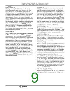
Component Value Selection
10,000(4-1/2 Digit)
1000(3-1/2 Digit)
× Clock Period × (20µA)
= -------------------------------------------------------------------------------------------------------------------------
For optimum performance of the analog section, care must
be taken in the selection of values for the integrator capacitor
and resistor, auto-zero capacitor, reference voltage, and
conversion rate. These values must be chosen to suit the
particular application.
C
INT
Integrator Output Voltage Swing
A very important characteristic of the integrating capacitor is
that it has low dielectric absorption to prevent roll-over or
ratiometric errors. A good test for dielectric absorption is to
use the capacitor with the input tied to the reference.
Integrating Resistor
This ratiometric condition should be read half scale 1.0000,
and any deviation is probably due to dielectric absorption.
Polypropylene capacitors give undetectable errors at
reasonable cost. Polystyrene and polycarbonate capacitors
may be used in less critical applications.
The integrating resistor is determined by the full scale input
voltage and the output current of the buffer used to charge
the integrator capacitor. This current should be small
compared to the output short circuit current such that
thermal effects are kept to a minimum and linearity is not
affected. Values of 5µA to 40µA give good results with a
nominal of 20µA. The exact value may be chosen by:
Auto-Zero and Reference Capacitor
The size of the auto-zero capacitor has some influence on
the noise of the system, with a larger value capacitor giving
less noise. The reference capacitor should be large enough
such that stray capacitance to ground from its nodes is
negligible.
Full Scale Voltage (See Note)
R
= ------------------------------------------------------------------------------
INT
20µA
NOTE: If gain is used in the buffer amplifier, then:
(BufferGain) (Full Scale Voltage)
R
= -------------------------------------------------------------------------------------------
INT
When gain is used in the buffer amplifier the reference
capacitor should be substantially larger than the auto-zero
capacitor. As a rule of thumb, the reference capacitor should
be approximately the gain times the value of the auto-zero
capacitor. The dielectric absorption of the reference cap and
auto-zero cap are only important at power-on or when the
circuit is recovering from an overload. Thus, smaller or
cheaper caps can be used here if accurate readings are not
required for the first few seconds of recovery.
20µA
Integrating Capacitor
The product of integrating resistor and capacitor is selected
to give 9V swing for full scale inputs. This is a compromise
between possibly saturating the integrator (at +14V) due to
tolerance buildup between the resistor, capacitor and clock
and the errors a lower voltage swing could induce due to
offsets referred to the output of the comparator. In general,
the value of C
is given by:
INT
10

 ETC [ ETC ]