ICL8052A/ICL71C03, ICL8068A/ICL71C03
A suitable circuit for driving a plasma-type display is shown
driver circuit could be ganged to the one shown if required.
This would be useful if additional annunciators were needed.
in Figure 8. The high voltage anode driver buffer is made by
Dionics. The 3 AND gates and caps driving “Bl” are needed
for interdigit blanking of multiple-digit display elements, and
can be omitted if not needed. The 2K and 3K resistors set
the current levels in the display. A similar arrangement can
be used with “Nixie” tubes.
1
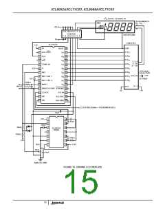
Figure 10 shows the complete circuit for a 4 /2 digit
( 2.000V) A/D, again using the internal reference of the
8052A/8068A.
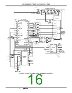
Figure 11 shows a more complicated circuit for driving LCD
displays. Here the data is latched into the ICM7211 by the
STROBE signal and “Overrange” is indicated by blanking the
4 digits. A clock oscillator circuit using the ICM7555 CMOS
timer is shown. Some other suitable clock circuits are
suggested in Figures 12 and 13. The 2-gate circuit should
use CMOS gates to maintain good power supply rejection.
Nixie is a registered trademark of Burroughs Corporation.
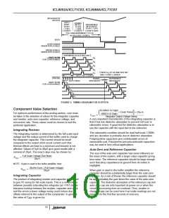
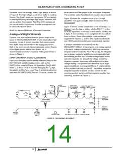
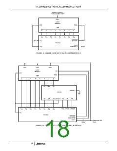
Analog and Digital Grounds
Extreme care must be taken to avoid ground loops in the
layout of 8068A or 8052A/71C03A circuits, especially in high
sensitivity circuits. It is most important that return currents
from digital loads are not fed into the analog ground line.
Both of the above circuits have considerable current flowing
in the digital ground returns from drivers, etc. A
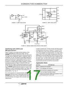
A problem sometimes encountered with the
8052A/68A/71C03 A/D is that of gross over-voltage applied
in the input. Voltage in excess of 2.000V may cause the
integrator output to saturate. When this occurs, the integrator
can no longer source (or sink) the current required to hold
the summing junction (Pin 11) at the voltage stored on the
auto zero capacitor. As a result, the voltage across the
integrator capacitor decreases sufficiently to give a false
voltage reading. This problem can also show up as large-
signal instability on overrange conditions. A simple solution
to this problem is to use junction FET transistors across the
integrator capacitor to source (or sink) current into the
summing junction and prevent the integrator amplifier from
saturating, as shown in Figure 14.
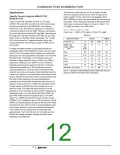
recommended connection sequence for the ground lines is
shown in Figure 9.
Other Circuits for Display Applications
Popular LCD displays can be interfaced to the Output of the
ICL71C03 with suitable display drivers, such as the
ICM7211A as shown in Figure 10. A standard CMOS 4000
1
series LCD driver circuit is used for displaying the / digit,
2
the polarity, and the “over-range” flag. A similar circuit can be
used with the ICM7212A LED driver. Of course, another full
REF
VOLTAGE
BUFF
OUT
EXTERNAL
REFERENCE
(IF USED)
ANALOG SUPPLY
BYPASS CAPACITORS
+15V
-15V
BUFF
-IN
(IF USED)
V
PIN 11
ICL71C03
AN GND
PIN 5
REF
I/P
FILTER
CAP
+
ICL8052A/68A
AN GND
V
C
IN
-
AZ
ANALOG
SUPPLY
RETURN
8068A PIN 2
COMPARATOR
BOARD
EDGE
DIGITAL
SUPPLY
RETURN
DIGITAL
LOGIC
DIG GND
ICL7104
PIN 2
DEVICE PIN
+5V SUPPLY BYPASS CAPACITOR(S)
FIGURE 9. GROUNDING SEQUENCE
14

 ETC [ ETC ]