ICL8052A/ICL71C03, ICL8068A/ICL71C03
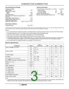
System Electrical Specifications: ICL8052A/ICL71C03
o
V++ = +15V, V+ = +5V, V- = -15V, T = 25 C, f
Set for 3 Reading/Sec. (Continued)
A
CLK
ICL8052A/ICL71C03
ICL8052A/A/ICL71C03
(NOTE 9)
(NOTE 10)
TEST
CONDITIONS
PARAMETER
MIN
TYP
MAX
MIN
TYP
MAX
UNITS
Differential Linearity (Difference between -2V ≤ V ≤ +2V
-
0.01
-
-
0.01
-
Counts
IN
Worst Case Step of Adjacent Counts and
Ideal Step)
Rollover Error (Difference in Reading for -V ≅ +V ≈ 2V
IN IN
-
0.2
1
-
0.5
1
Counts
Equal Positive & Negative Voltage Near
Full Scale)
Noise (Peak-To-Peak Value Not
Exceeded 95% of Time)
V
= 0V,
IN
Full Scale = 200mV,
Full Scale = 2V
-
20
50
-
-
-
-
-
-
µV
30
3
Leakage Current at Input
Zero Reading Drift
V
= 0V
-
-
5
1
30
5
-
-
10
2
pA
IN
IN
o
V
= 0V,
0.5
µV/ C
o
o
0 C To 70 C
o
Scale Factor Temperature Coefficient
V
= 2V,
-
3
15
-
2
5
ppm/ C
IN
o
o
0 C To 70 C,
Ext. Ref. 0ppm/ C
o
NOTES:
1
10. Tested in 3 / digit (2,000 count) circuit shown in Figure 5, clock frequency 12kHz. Pin 2 71C03 connected to GND.
2
1
11. Tested in 4 / digit (20,000 count) circuit shown in Figure 5, clock frequency 120kHz. Pin 2 71C03A open.
2
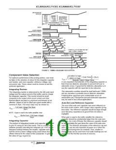
12. Tested with a low dielectric absorption integrating capacitor. See Component Selection Section.
o
13. The temperature range can be extended to 70 C and beyond if the Auto-Zero and Reference capacitors are increased to absorb the high
temperature leakage of the 8068A.
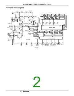
Zero phase, and the integrator will generate a ramp whose
Detailed Description
slope is proportional to V . At the end of this phase, the
IN
Analog Section
sign of the ramp is latched into the polarity F/F.
Figure 2 shows the equivalent Circuit of the Analog Section
of both the ICL71C03/8052A and the ICL71C03/8068A in
the 3 different phases of operation. IF the RUN/HOLD pin is
Deintegrate Phase II (Figures 2C and 2D)
During the Deintegrate phase, the switch drive logic uses the
output of the polarity F/F in determining whether to close
switch 6 or 5. If the input signal is positive, switch 6 is closed
left open or tied to V+, the system will perform conversions
1
at a rate determined by the clock frequency: 40,0002 at 4 /
1
2
and a voltage which is V
more negative than during
digit and 4002 at 3 / digit clock periods per cycle (see
2
REF
Auto-Zero is impressed on the BUFFER INPUT. Negative
Inputs will cause +2(V ) to be applied to the BUFFER
Figure 3 for details of conversion timing).
REF
Auto-Zero Phase I (Figure 2A)
INPUT via switch 5. Thus, the reference capacitor generates
the equivalent of a (+) or (-) reference from the single
reference voltage with negligible error. The reference voltage
returns the output of the integrator to the zero-crossing point
established in Phase I. The time, or number of counts,
required to do this is proportional to the input voltage. Since
the Deintegrate phase can be twice as long as the Input
Integrate Phase, the input voltage required to give a full
During the Auto-Zero, the input of the buffer is connected to
through switch 2, and switch 3 closes a loop around
V
REF
the integrator and comparator, the purpose of which is to
charge the auto-zero capacitor until the integrator output
does not change with time. Also, switches 1 and 2 recharge
the reference capacitor to V
.
REF
Input Integrate Phase II (Figure 2B)
scale reading is 2V
.
REF
During Input Integrate the auto-zero loop is opened and the
ANALOG INPUT is connected to the BUFFER INPUT
through switch 4 and C
. If the input signal is zero, the
REF
buffer, integrator and comparator will see the same voltage
that existed in the previous state (Auto-Zero). Thus, the
integrator output will not change but will remain stationary
during the entire Input Integrate cycle. If V is not equal to
IN
zero, and unbalanced condition exists compared to the Auto
6

 ETC [ ETC ]