ST72104G, ST72215G, ST72216G, ST72254G
2
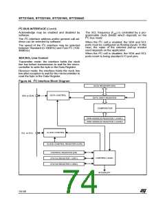
I C BUS INTERFACE (Cont’d)
Acknowledge may be enabled and disabled by
software.
The SCL frequency (F ) is controlled by a pro-
scl
grammable clock divider which depends on the
2
2
I C bus mode.
The I C interface address and/or general call ad-
2
dress can be selected by software.
When the I C cell is enabled, the SDA and SCL
2
ports must be configured as floating inputs. In this
case, the value of the external pull-up resistor
used depends on the application.
The speed of the I C interface may be selected
2
between Standard (0-100KHz) and Fast I C (100-
400KHz).
2
When the I C cell is disabled, the SDA and SCL
ports revert to being standard I/O port pins.
SDA/SCL Line Control
Transmitter mode: the interface holds the clock
line low before transmission to wait for the micro-
controller to write the byte in the Data Register.
Receiver mode: the interface holds the clock line
low after reception to wait for the microcontroller to
read the byte in the Data Register.
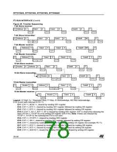
2
Figure 44. I C Interface Block Diagram
DATA REGISTER (DR)
DATA CONTROL
SDA or SDAI
DATA SHIFT REGISTER
COMPARATOR
OWN ADDRESS REGISTER 1 (OAR1)
OWN ADDRESS REGISTER 2 (OAR2)
CLOCK CONTROL
SCL or SCLI
CLOCK CONTROL REGISTER (CCR)
CONTROL REGISTER (CR)
STATUS REGISTER 1 (SR1)
STATUS REGISTER 2 (SR2)
CONTROL LOGIC
INTERRUPT
74/140

 ETC [ ETC ]