ST72104G, ST72215G, ST72216G, ST72254G
SERIAL PERIPHERAL INTERFACE (Cont’d)
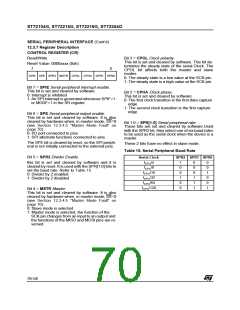
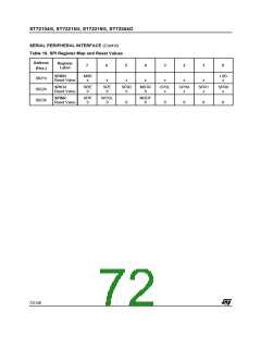
STATUS REGISTER (SR)
Read Only
DATA I/O REGISTER (DR)
Read/Write
Reset Value: 0000 0000 (00h)
Reset Value: Undefined
7
0
-
7
0
SPIF
WCOL
-
MODF
-
-
-
D7
D6
D5
D4
D3
D2
D1
D0
Bit 7 = SPIF Serial Peripheral data transfer flag.
This bit is set by hardware when a transfer has
been completed. An interrupt is generated if
SPIE=1 in the CR register. It is cleared by a soft-
ware sequence (an access to the SR register fol-
lowed by a read or write to the DR register).
0: Data transfer is in progress or has been ap-
proved by a clearing sequence.
The DR register is used to transmit and receive
data on the serial bus. In the master device only a
write to this register will initiate transmission/re-
ception of another byte.
Notes: During the last clock cycle the SPIF bit is
set, a copy of the received data byte in the shift
register is moved to a buffer. When the user reads
the serial peripheral data I/O register, the buffer is
actually being read.
1: Data transfer between the device and an exter-
nal device has been completed.
Warning:
Note: While the SPIF bit is set, all writes to the DR
register are inhibited.
A write to the DR register places data directly into
the shift register for transmission.
A write to the the DR register returns the value lo-
cated in the buffer and not the contents of the shift
register (See Figure 38 ).
Bit 6 = WCOL Write Collision status.
This bit is set by hardware when a write to the DR
register is done during a transmit sequence. It is
cleared by a software sequence (see Figure 41).
0: No write collision occurred
1: A write collision has been detected
Bit 5 = Unused.
Bit 4 = MODF Mode Fault flag.
This bit is set by hardware when the SS pin is
pulled low in master mode (see Section 12.3.4.5
"Master Mode Fault" on page 70). An SPI interrupt
can be generated if SPIE=1 in the CR register.
This bit is cleared by a software sequence (An ac-
cess to the SR register while MODF=1 followed by
a write to the CR register).
0: No master mode fault detected
1: A fault in master mode has been detected
Bits 3-0 = Unused.
71/140

 ETC [ ETC ]