ST72104G, ST72215G, ST72216G, ST72254G
SERIAL PERIPHERAL INTERFACE (Cont’d)
12.3.7 Register Description
CONTROL REGISTER (CR)
Read/Write
Bit 3 = CPOL Clock polarity.
This bit is set and cleared by software. This bit de-
termines the steady state of the serial Clock. The
CPOL bit affects both the master and slave
modes.
Reset Value: 0000xxxx (0xh)
7
0
SPIE SPE SPR2 MSTR CPOL CPHA SPR1 SPR0
0: The steady state is a low value at the SCK pin.
1: The steady state is a high value at the SCK pin.
Bit 7 = SPIE Serial peripheral interrupt enable.
This bit is set and cleared by software.
0: Interrupt is inhibited
1: An SPI interrupt is generated whenever SPIF=1
or MODF=1 in the SR register
Bit 2 = CPHA Clock phase.
This bit is set and cleared by software.
0: The first clock transition is the first data capture
edge.
1: The second clock transition is the first capture
edge.
Bit 6 = SPE Serial peripheral output enable.
This bit is set and cleared by software. It is also
cleared by hardware when, in master mode, SS=0
(see Section 12.3.4.5 "Master Mode Fault" on
page 70).
0: I/O port connected to pins
1: SPI alternate functions connected to pins
Bit 1:0 = SPR[1:0] Serial peripheral rate.
These bits are set and cleared by software.Used
with the SPR2 bit, they select one of six baud rates
to be used as the serial clock when the device is a
master.
The SPE bit is cleared by reset, so the SPI periph-
eral is not initially connected to the external pins.
These 2 bits have no effect in slave mode.
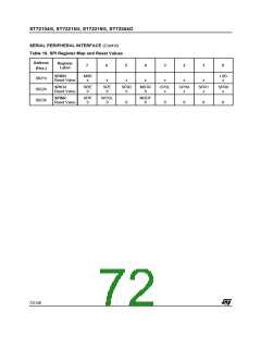
Table 15. Serial Peripheral Baud Rate
Bit 5 = SPR2 Divider Enable.
Serial Clock
SPR2 SPR1 SPR0
this bit is set and cleared by software and it is
cleared by reset. It is used with the SPR[1:0] bits to
set the baud rate. Refer to Table 15.
0: Divider by 2 enabled
f
f
/4
/8
1
0
0
1
0
0
0
0
0
1
1
1
0
0
1
0
0
1
CPU
CPU
f
f
f
/16
/32
/64
CPU
CPU
CPU
1: Divider by 2 disabled
f
/128
CPU
Bit 4 = MSTR Master.
This bit is set and cleared by software. It is also
cleared by hardware when, in master mode, SS=0
(see Section 12.3.4.5 "Master Mode Fault" on
page 70).
0: Slave mode is selected
1: Master mode is selected, the function of the
SCK pin changes from an input to an output and
the functions of the MISO and MOSI pins are re-
versed.
70/140

 ETC [ ETC ]