ST72104G, ST72215G, ST72216G, ST72254G
SERIAL PERIPHERAL INTERFACE (Cont’d)
12.3.4.4 Write Collision Error
When the CPHA bit is reset:
A write collision occurs when the software tries to
write to the DR register while a data transfer is tak-
ing place with an external device. When this hap-
pens, the transfer continues uninterrupted; and
the software write will be unsuccessful.
Data is latched on the occurrence of the first clock
transition. The slave device does not have any
way of knowing when that transition will occur;
therefore, the slave device collision occurs when
software attempts to write the DR register after its
SS pin has been pulled low.
Write collisions can occur both in master and slave
mode.
For this reason, the SS pin must be high, between
each data byte transfer, to allow the CPU to write
in the DR register without generating a write colli-
sion.
Note: a "read collision" will never occur since the
received data byte is placed in a buffer in which
access is always synchronous with the MCU oper-
ation.
In Slave mode
In Master mode
When the CPHA bit is set:
Collision in the master device is defined as a write
of the DR register while the internal serial clock
(SCK) is in the process of transfer.
The slave device will receive a clock (SCK) edge
prior to the latch of the first data transfer. This first
clock edge will freeze the data in the slave device
DR register and output the MSBit on to the exter-
nal MISO pin of the slave device.
The SS pin signal must be always high on the
master device.
The SS pin low state enables the slave device but
the output of the MSBit onto the MISO pin does
not take place until the first data transfer clock
edge.
WCOL bit
The WCOL bit in the SR register is set if a write
collision occurs.
No SPI interrupt is generated when the WCOL bit
is set (the WCOL bit is a status flag only).
Clearing the WCOL bit is done through a software
sequence (see Figure 41).
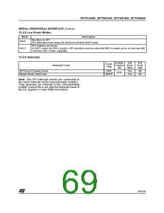
Figure 41. Clearing the WCOL bit (Write Collision Flag) Software Sequence
Clearing sequence after SPIF = 1 (end of a data byte transfer)
Read SR
Read SR
1st Step
2nd Step
OR
THEN
THEN
SPIF =0
WCOL=0
SPIF =0
WCOL=0 if no transfer has started
WCOL=1 if a transfer has started
before the 2nd step
Read DR
Write DR
Clearing sequence before SPIF = 1 (during a data byte transfer)
Read SR
1st Step
THEN
Note: Writing in DR register in-
2nd Step
Read DR
stead of reading in it do not reset
WCOL bit
WCOL=0
66/140

 ETC [ ETC ]