ST72104G, ST72215G, ST72216G, ST72254G
SERIAL PERIPHERAL INTERFACE (Cont’d)
12.3.4.3 Data Transfer Format
The master device applies data to its MOSI pin-
clock edge before the capture clock edge.
During an SPI transfer, data is simultaneously
transmitted (shifted out serially) and received
(shifted in serially). The serial clock is used to syn-
chronize the data transfer during a sequence of
eight clock pulses.
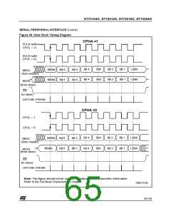
CPHA bit is set
The second edge on the SCK pin (falling edge if
the CPOL bit is reset, rising edge if the CPOL bit is
set) is the MSBit capture strobe. Data is latched on
the occurrence of the second clock transition.
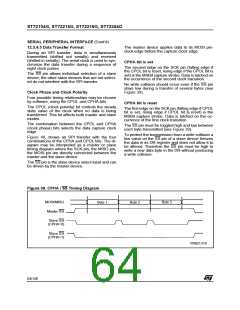
The SS pin allows individual selection of a slave
device; the other slave devices that are not select-
ed do not interfere with the SPI transfer.
No write collision should occur even if the SS pin
stays low during a transfer of several bytes (see
Figure 39).
Clock Phase and Clock Polarity
Four possible timing relationships may be chosen
by software, using the CPOL and CPHA bits.
CPHA bit is reset
The CPOL (clock polarity) bit controls the steady
state value of the clock when no data is being
transferred. This bit affects both master and slave
modes.
The first edge on the SCK pin (falling edge if CPOL
bit is set, rising edge if CPOL bit is reset) is the
MSBit capture strobe. Data is latched on the oc-
currence of the first clock transition.
The combination between the CPOL and CPHA
(clock phase) bits selects the data capture clock
edge.
The SS pin must be toggled high and low between
each byte transmitted (see Figure 39).
To protect the transmission from a write collision a
low value on the SS pin of a slave device freezes
the data in its DR register and does not allow it to
be altered. Therefore the SS pin must be high to
write a new data byte in the DR without producing
a write collision.
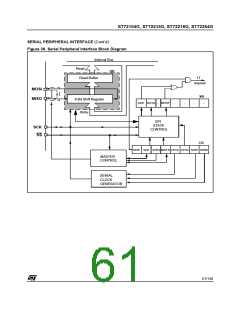
Figure 40, shows an SPI transfer with the four
combinations of the CPHA and CPOL bits. The di-
agram may be interpreted as a master or slave
timing diagram where the SCK pin, the MISO pin,
the MOSI pin are directly connected between the
master and the slave device.
The SS pin is the slave device select input and can
be driven by the master device.
Figure 39. CPHA / SS Timing Diagram
Byte 3
Byte 2
MOSI/MISO
Byte 1
Master SS
Slave SS
(CPHA=0)
Slave SS
(CPHA=1)
VR02131A
64/140

 ETC [ ETC ]