ST72104G, ST72215G, ST72216G, ST72254G
SERIAL PERIPHERAL INTERFACE (Cont’d)
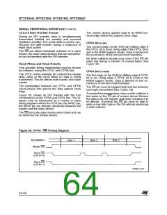
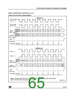
Figure 40. Data Clock Timing Diagram
CPHA =1
SCLK (with
CPOL = 1)
SCLK (with
CPOL = 0)
Bit 4
Bit 4
Bit3
Bit3
Bit 2
Bit 2
Bit 1
Bit 1
LSBit
LSBit
MSBit
MSBit
Bit 6
Bit 6
Bit 5
Bit 5
MISO
(from master)
MOSI
(from slave)
SS
(to slave)
CAPTURE STROBE
CPHA =0
CPOL = 1
CPOL = 0
Bit 4
Bit 4
Bit3
Bit 2
Bit 2
Bit 1
Bit 1
LSBit
LSBit
MSBit
Bit 6
Bit 6
Bit 5
Bit 5
MISO
(from master)
MSBit
Bit3
MOSI
(from slave)
SS
(to slave)
CAPTURE STROBE
Note: This figure should not be used as a replacement for parametric information.
Refer to the Electrical Characteristics chapter.
VR02131B
65/140

 ETC [ ETC ]