ST72104G, ST72215G, ST72216G, ST72254G
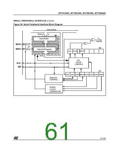
SERIAL PERIPHERAL INTERFACE (Cont’d)
12.3.4.2 Slave Configuration
When data transfer is complete:
– The SPIF bit is set by hardware
In slave configuration, the serial clock is received
on the SCK pin from the master device.
– An interrupt is generated if SPIE bit is set and
I bit in CCR register is cleared.
The value of the SPR0 & SPR1 bits is not used for
the data transfer.
During the last clock cycle the SPIF bit is set, a
copy of the data byte received in the shift register
is moved to a buffer. When the DR register is read,
the SPI peripheral returns this buffered value.
Procedure
– For correct data transfer, the slave device
must be in the same timing mode as the mas-
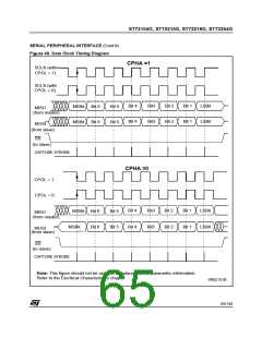
ter device (CPOL and CPHA bits). See Figure
40.
Clearing the SPIF bit is performed by the following
software sequence:
1. An access to the SR register while the SPIF bit
is set.
– The SS pin must be connected to a low level
signal during the complete byte transmit se-
quence.
2.A read to the DR register.
– Clear the MSTR bit and set the SPE bit to as-
sign the pins to alternate function.
Notes: While the SPIF bit is set, all writes to the
DR register are inhibited until the SR register is
read.
In this configuration the MOSI pin is a data input
and the MISO pin is a data output.
The SPIF bit can be cleared during a second
transmission; however, it must be cleared before
the second SPIF bit in order to prevent an overrun
condition (see Section 12.3.4.6).
Transmit Sequence
The data byte is parallel loaded into the 8-bit shift
register (from the internal bus) during a write cycle
and then shifted out serially to the MISO pin most
significant bit first.
Depending on the CPHA bit, the SS pin has to be
set to write to the DR register between each data
byte transfer to avoid a write collision (see Section
12.3.4.4).
The transmit sequence begins when the slave de-
vice receives the clock signal and the most signifi-
cant bit of the data on its MOSI pin.
63/140

 ETC [ ETC ]