ST6200C/ST6201C/ST6203C
RESET (Cont’d)
5.3.3 RESET Pin
If the RESET pin is grounded while the MCU is in
RUN or WAIT modes, processing of the user pro-
gram is stopped (RUN mode only), the I/O ports
are configured as inputs with pull-up resistors and
the main oscillator is restarted. When the level on
the RESET pin then goes high, the initialization se-
quence is executed at the end of the internal delay
period.
The RESET pin may be connected to a device on
the application board in order to reset the MCU if
required. The RESET pin may be pulled low in
RUN, WAIT or STOP mode. This input can be
used to reset the internal state of the MCU and en-
sure it starts-up correctly. The pin, which is con-
nected to an internal pull-up, is active low and fea-
tures a Schmitt trigger input. A delay (2048 clock
cycles) added to the external signal ensures that
even short pulses on the RESET pin are accepted
If the RESET pin is grounded while the MCU is in
STOP mode, the oscillator starts up and all the I/O
ports are configured as inputs with pull-up resis-
tors. When the RESET pin level then goes high,
the initialization sequence is executed at the end
of the internal delay period.
as valid, provided V
has completed its rising
DD
phase and that the oscillator is running correctly
(normal RUN or WAIT modes). The MCU is kept in
the Reset state as long as the RESET pin is held
low.
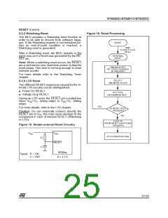
A simple external RESET circuitry is shown in Fig-
ure 15. For more details, please refer to the appli-
cation note AN669.
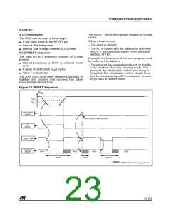
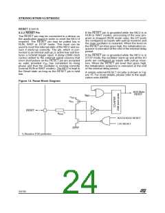
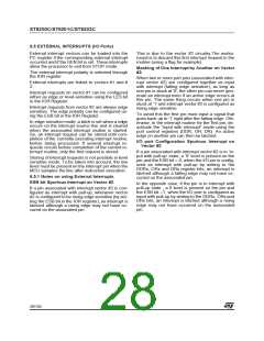
Figure 14. Reset Block Diagram
INTERNAL
RESET
f
INT
V
DD
R
PU
RESET
1)
R
ESD
WATCHDOG RESET
LVD RESET
1) Resistive ESD protection
24/104
1

 ETC [ ETC ]