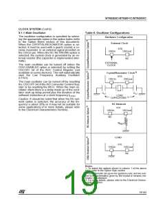
ST6200C/ST6201C/ST6203C
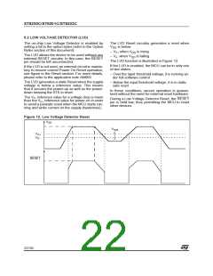
5.3 RESET
5.3.1 Introduction
The RESET vector fetch phase duration is 2 clock
cycles.
The MCU can be reset in three ways:
■ A low pulse input on the RESET pin
■ Internal Watchdog reset
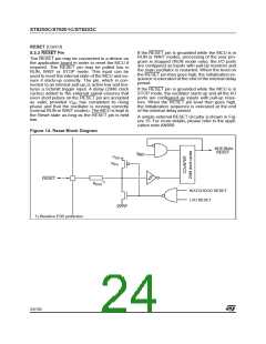
When a reset occurs:
– The stack is cleared
– The PC is loaded with the address of the Reset
vector. It is located in program ROM starting at
address 0FFEh.
■ Internal Low Voltage Detector (LVD) reset
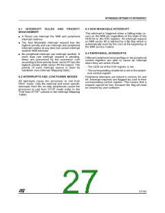
5.3.2 RESET sequence
The basic RESET sequence consists of 3 main
phases:
■ Internal (watchdog or LVD) or external Reset
A jump to the beginning of the user program must
be coded at this address.
– Theinterrupt flag is automatically set, so that the
CPU is in Non Maskable Interrupt mode. This
prevents the initialization routine from being in-
terrupted. The initialization routine should there-
fore be terminated by a RETI instruction, in order
to go back to normal mode.
event
■ A delay of 2048 clock (f ) cycles
INT
■ RESET vector fetch
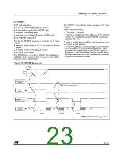
The 2048 clock cycle delay allows the oscillator to
stabilise and ensures that recovery has taken
place from the Reset state.
Figure 13. RESET Sequence
V
DD
V
V
IT+
IT-
WATCHDOG
RESET
WATCHDOG UNDERFLOW
LVD
RESET
RESET PIN
INTERNAL
RESET
RUN
RUN
RUN
RUN
RESET
RESET
RESET
2048 CLOCK CYCLE (f
) DELAY
INT
23/104
1

 ETC [ ETC ]