PIC12F510/16F506
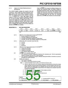
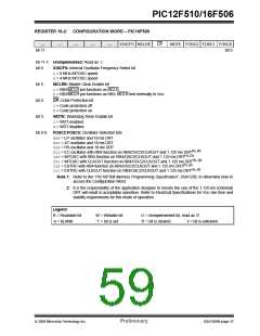
REGISTER 10-2: CONFIGURATION WORD – PIC16F506
—
—
—
—
—
IOSCFS MCLRE
CP
WDTE FOSC2 FOSC1 FOSC0
bit 0
bit 11
bit 11-7: Unimplemented: Read as ‘1’
bit 6:
bit 5:
bit 4:
bit 3:
IOSCFS: Internal Oscillator Frequency Select bit
1= 8 MHz INTOSC speed
0= 4 MHz INTOSC speed
MCLRE: Master Clear Enable bit
1= RB3/MCLR pin functions as MCLR
0= RB3/MCLR pin functions as RB3, MCLR tied internally to VDD
CP: Code Protection bit
1= Code protection off
0= Code protection on
WDTE: Watchdog Timer Enable bit
1= WDT enabled
0= WDT disabled
bit 2-0: FOSC2:FOSC0: Oscillator Selection bits
000= LP oscillator and 18 ms DRT
001= XT oscillator and 18 ms DRT
010= HS oscillator and 18 ms DRT
011= EC oscillator with RB4 function on RB4/OSC2/CLKOUT and 1.125 ms DRT(1), (2)
100= INTOSC with RB4 function on RB4/OSC2/CLKOUT and 1.125 ms DRT(1), (2)
101= INTOSC with CLKOUT function on RB4/OSC2/CLKOUT and 1.125 ms DRT(1), (2)
110= EXTRC with RB4 function on RB4/OSC2/CLKOUT and 1.125 ms DRT(1), (2)
111= EXTRC with CLKOUT function on RB4/OSC2/CLKOUT and 1.125 ms DRT(1), (2)
Note 1: Refer to the “PIC16F506 Memory Programming Specification”, DS41258, to determine how to
access the Configuration Word.
2: It is the responsibility of the application designer to ensure the use of the 1.125 ms (nominal)
DRT will result in acceptable operation. Refer to Electrical Specifications for VDD rise time and
stability requirements for this mode of operation.
Legend:
R = Readable bit
-n = bLANK
W = Writable bit
‘1’ = bit is set
U = Unimplemented bit, read as ‘0’
‘0’ = bit is cleared x = bit is unknown
© 2006 Microchip Technology Inc.
Preliminary
DS41268B-page 57

 ETC [ ETC ]