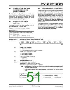
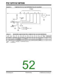
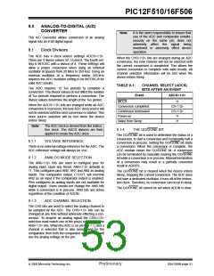
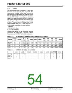
PIC12F510/16F506
If the GO/DONE bit is cleared in software during a con-
version, the conversion stops. The data in ADRES is
the partial conversion result. This data is valid for the bit
weights that have been converted. The position of the
‘leading one’ determines the number of bits that have
been converted. The bits that were not converted
before the GO/DONE was cleared are unrecoverable.
9.1.6
ANALOG CONVERSION RESULT
REGISTER
The ADRES register contains the results of the last
conversion. These results are present during the sam-
pling period of the next analog conversion process.
After the sampling period is over, ADRES is cleared
(= 0). A ‘leading one’ is then right shifted into the
ADRES to serve as an internal conversion complete
bit. As each bit weight, starting with the MSB, is con-
verted, the leading one is shifted right and the con-
verted bit is stuffed into ADRES. After a total of 9 right
shifts of the ‘leading one’ have taken place, the conver-
sion is complete; the ‘leading one’ has been shifted out
and the GO/DONE bit is cleared.
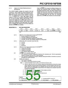
REGISTER 9-1:
ADCON0 REGISTER
R/W-1
R/W-1
R/W-1
R/W-1
R/W-1
CHS1
R/W-1
CHS0
R/W-0
R/W-0
ADON
ANS1
ANS0
ADCS1
ADCS0
GO/DONE
bit 7
bit 0
(1), (2), (3), (6)
bit 7-6
bit 5-4
bit 3-2
bit 1
ANS<1:0>: ADC Analog Input Pin Select bits
00= No pins configured for analog input
01= GP2/AN2 configured as an analog input
10= GP2/AN2 and GP0/AN0 configured as analog inputs
11= GP2/AN2, GP1/AN1 and GP0/AN0 configured as analog inputs
ADCS<1:0>: ADC Conversion Clock Select bits
00= FOSC/32
01= FOSC/16
10= FOSC/8
11= INTOSC/8
(4), (6)
CHS<1:0>: ADC Channel Select bits for PIC16F506
00= Channel 00 (GP0/AN0)
01= Channel 01 (GP1/AN1)
10= Channel 02 (GP2/AN2)
11= 0.6V absolute voltage reference
(5)
GO/DONE: ADC Conversion Status bit
1= ADC conversion in progress. Setting this bit starts an ADC conversion cycle. This bit is automatically
cleared by hardware when the ADC is done converting.
0= ADC conversion completed/not in progress. Manually clearing this bit while a conversion is in process
terminates the current conversion.
bit 0
ADON: ADC Enable bit
1= ADC module is operating
0= ADC module is shut-off and consumes no power
Note 1: On the PIC16F506, the term is RBx, on PIC12F510, the term is GPx.
2: When the ANS bits are set, the channels selected will automatically be forced into Analog
mode, regardless of the pin function previously defined. The only exception to this is the com-
parator, where the analog input to the comparator and the ADC will be active at the same
time. It is the users responsibility to ensure that the ADC loading on the comparator input does
not affect their application.
3: The ANS<1:0> bits are active regardless of the condition of ADON.
4: CHS<1:0> bits default to 11after any Reset.
5: If the ADON bit is clear, the GO/DONE bit cannot be set.
6: C1OUT, when enabled, overrides AN2.
Legend:
R = Readable bit
-n = Value at POR
W = Writable bit
‘1’ = Bit is set
U = Unimplemented bit, read as ‘0’
‘0’ = Bit is cleared x = Bit is unknown
© 2006 Microchip Technology Inc.
Preliminary
DS41268B-page 53

 ETC [ ETC ]