PIC12F510/16F506
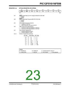
4.2.2
SPECIAL FUNCTION REGISTERS
The Special Function Registers (SFRs) are registers
used by the CPU and peripheral functions to control the
operation of the device (see Table 4-1).
The Special Function Registers can be classified into
two sets. The Special Function Registers associated
with the “core” functions are described in this section.
Those related to the operation of the peripheral
features are described in the section for each
peripheral feature.
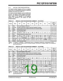
TABLE 4-1:
SPECIAL FUNCTION REGISTER SUMMARY – PIC12F510
Value on
Address
Name
Bit 7
Bit 6
Bit 5
Bit 4
Bit 3
Bit 2
Bit 1
Bit 0
Power-on
Reset
N/A
N/A
00h
01h
02h
TRIS
I/O Control Registers (TRISGPIO)
--11 1111
1111 1111
xxxx xxxx
xxxx xxxx
1111 1111
OPTION
INDF
Contains control bits to configure Timer0 and Timer0/WDT Prescaler
Uses contents of FSR to address data memory (not a physical register)
Timer0 Module Register
TMR0
PCL
(1)
Low Order 8 bits of PC
03h
STATUS
GPWUF
CWUF
PA0
TO
PD
Z
DC
C
0001 1xxx
100x xxxx
04h
05h
06h
FSR
Indirect Data Memory Address Pointer
OSCCAL
GPIO
CAL6
—
CAL5
—
CAL4
GP5
CAL3
GP4
CAL2
GP3
CAL1
GP2
CAL0
GP1
—
1111 111-
--xx xxxx
GP0
07h
CM1CON0
C1OUT
ANS1
C1OUTEN C1POL
ANS0 ADCS1
C1T0CS
ADCS0
C1ON
CHS1
C1NREF
CHS0
C1PREF
C1WU
ADON
1111 1111
08h
09h
ADCON0
ADRES
GO/DONE
1111 1100
xxxx xxxx
ADC Conversion Result
Legend:
Note 1:
x= unknown, u= unchanged, – = unimplemented, read as ‘0’ (if applicable). Shaded cells = unimplemented or unused.
The upper byte of the Program Counter is not directly accessible. See Section 4.6 “Program Counter” for an explanation of
how to access these bits.
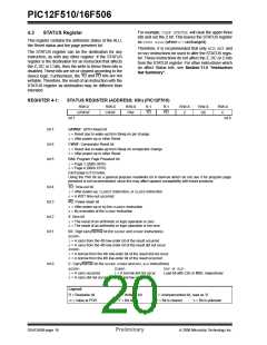
TABLE 4-2:
SPECIAL FUNCTION REGISTER SUMMARY – PIC16F506
Value on
Power-on
Reset
Address
Name
Bit 7
Bit 6
Bit 5
Bit 4
Bit 3
Bit 2
Bit 1
Bit 0
N/A
N/A
00h
01h
02h
TRIS
I/O Control Registers (TRISB, TRISC)
--11 1111
1111 1111
xxxx xxxx
xxxx xxxx
1111 1111
OPTION
INDF
Contains control bits to configure Timer0 and Timer0/WDT Prescaler
Uses contents of FSR to address data memory (not a physical register)
Timer0 Module Register
TMR0
PCL
(1)
Low Order 8 bits of PC
03h
04h
05h
06h
07h
STATUS
FSR
RBWUF
CWUF
PA0
TO
PD
Z
DC
C
0001 1xxx
100x xxxx
1111 111-
--xx xxxx
--xx xxxx
Indirect Data Memory Address Pointer
OSCCAL
PORTB
PORTC
CAL6
—
CAL5
—
CAL4
RB5
CAL3
RB4
CAL2
RB3
CAL1
RB2
CAL0
RB1
—
RB0
RC0
—
—
RC5
RC4
RC3
RC2
RC1
08h
09h
CM1CON0
C1OUT
ANS1
C1OUTEN
ANS0
C1POL
ADCS1
C1T0CS
ADCS0
C1ON
CHS1
C1NREF
CHS0
C1PREF
C1WU
ADON
1111 1111
ADCON0
ADRES
GO/DONE
1111 1100
xxxx xxxx
0Ah
ADC Conversion Result
0Bh
0Ch
CM2CON0
VRCON
C2OUT
VREN
C2OUTEN
VROE
C2POL
VRR
C2PREF2
—
C2ON
VR3
C2NREF
VR2
C2PREF1
VR1
C2WU
VR0
1111 1111
001- 1111
Legend:
Note 1:
x= unknown, u= unchanged, – = unimplemented, read as ‘0’ (if applicable). Shaded cells = unimplemented or unused.
The upper byte of the Program Counter is not directly accessible. See Section 4.6 “Program Counter” for an explanation of
how to access these bits.
© 2006 Microchip Technology Inc.
Preliminary
DS41268B-page 17

 ETC [ ETC ]