PIC12F510/16F506
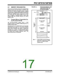
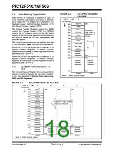
FIGURE 4-2:
PIC12F510 REGISTER
FILE MAP
4.2
Data Memory Organization
Data memory is composed of registers or bytes of
RAM. Therefore, data memory for a device is specified
by its register file. The register file is divided into two
functional groups: Special Function Registers (SFR)
and General Purpose Registers (GPR).
FSR<5>
File Address
00h
0
1
INDF(1)
TMR0
20h
01h
02h
03h
04h
05h
06h
The Special Function Registers include the TMR0
register, the Program Counter (PCL), the STATUS
register, the I/O registers (ports) and the File Select
Register (FSR). In addition, Special Function Registers
are used to control the I/O port configuration and
prescaler options.
PCL
Addresses
map back to
addresses in
Bank 0.
STATUS
FSR
OSCCAL
GPIO
The General Purpose Registers are used for data and
control information under command of the instructions.
CM1CON0
07h
08h
ADCON0
ADRES
For the PIC12F510, the register file is composed of 10
Special Function Registers,
Registers and 32 General Purpose Registers accessed
by banking (see Figure 4-2).
09h
0Ah
6 General Purpose
General
Purpose
Registers
0Fh
10h
2Fh
30h
For the PIC16F506, the register file is composed of 13
Special Function Registers,
3 General Purpose
General
Purpose
Registers
General
Purpose
Registers
Registers and 64 General Purpose Registers accessed
by banking (see Figure 4-3).
4.2.1
GENERAL PURPOSE REGISTER
FILE
1Fh
3Fh
The General Purpose Register file is accessed either
directly or indirectly through the File Select Register
(FSR). See Section 4.8 “Indirect Data Addressing:
INDF and FSR Registers”.
Bank 0
Bank 1
Note 1: Not a physical register.
FIGURE 4-3:
PIC16F506 REGISTER FILE MAP
FSR<6:5>
File Address
00h
00
01
10
11
INDF(1)
TMR0
20h
40h
60h
01h
02h
PCL
03h
04h
STATUS
FSR
OSCCAL
05h
06h
07h
Addresses map back to
addresses in Bank 0.
PORTB
PORTC
CM1CON0
ADCON0
ADRES
08h
09h
0Ah
CM2CON0
VRCON
0Bh
0Ch
0Dh
General
Purpose
Registers
0Fh
10h
2Fh
30h
4Fh
50h
6Fh
70h
General
Purpose
Registers
General
Purpose
Registers
General
Purpose
Registers
General
Purpose
Registers
5Fh
7Fh
1Fh
3Fh
Bank 0
Bank 1
Bank 2
Bank 3
Note 1: Not a physical register.
DS41268B-page 16
Preliminary
© 2006 Microchip Technology Inc.

 ETC [ ETC ]