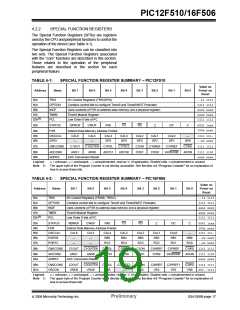
PIC12F510/16F506
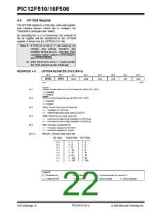
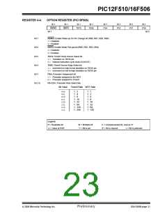
REGISTER 4-4:
OPTION REGISTER (PIC16F506)
W-1
W-1
W-1
W-1
W-1
W-1
PS2
W-1
PS1
W-1
PS0
RBWU
RBPU
T0CS
T0SE
PSA
bit 7
bit 0
bit 7
bit 6
bit 5
bit 4
bit 3
bit 2-0
RBWU: Enable Wake-up On Pin Change bit (RB0, RB1, RB3, RB4)
1= Disabled
0= Enabled
RBPU: Enable Weak Pull-ups bit (RB0, RB1, RB3, RB4)
1= Disabled
0= Enabled
T0CS: Timer0 Clock Source Select bit
1= Transition on T0CKI pin
0= Internal instruction cycle clock (CLKOUT)
T0SE: Timer0 Source Edge Select bit
1= Increment on high-to-low transition on T0CKI pin
0= Increment on low-to-high transition on T0CKI pin
PSA: Prescaler Assignment bit
1= Prescaler assigned to the WDT
0= Prescaler assigned to Timer0
PS<2:0>: Prescaler Rate Select bits
Bit Value
Timer0 Rate WDT Rate
000
001
010
011
100
101
110
111
1 : 2
1 : 4
1 : 8
1 : 16
1 : 32
1 : 64
1 : 128
1 : 256
1 : 1
1 : 2
1 : 4
1 : 8
1 : 16
1 : 32
1 : 64
1 : 128
Legend:
R = Readable bit
-n = Value at POR
W = Writable bit
‘1’ = Bit is set
U = Unimplemented bit, read as ‘0’
‘0’ = Bit is cleared x = Bit is unknown
© 2006 Microchip Technology Inc.
Preliminary
DS41268B-page 21

 ETC [ ETC ]