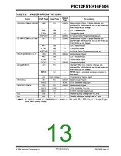
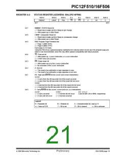
PIC12F510/16F506
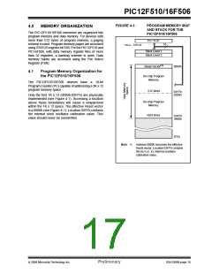
FIGURE 4-1:
PROGRAM MEMORY MAP
AND STACK FOR THE
PIC12F510/16F506
4.0
MEMORY ORGANIZATION
The PIC12F510/16F506 memories are organized into
program memory and data memory. For devices with
more than 512 bytes of program memory, a paging
scheme is used. Program memory pages are accessed
using STATUS register bit PA0. For the PIC12F510 and
PIC16F506, with data memory register files of more
than 32 registers, a banking scheme is used. Data
memory banks are accessed using the File Select
Register (FSR).
PC<11:0>
10
CALL, RETLW
Stack Level 1
Stack Level 2
(1)
Reset Vector
0000h
4.1
Program Memory Organization for
the PIC12F510/16F506
On-chip Program
Memory
The PIC12F510/16F506 devices have
a
10-bit
Program Counter (PC) capable of addressing a 2K x 12
program memory space.
512 Word
01FFh
0200h
Only the first 1K x 12 (0000h-03FFh) are physically
implemented (see Figure 4-1). Accessing a location
above these boundaries will cause a wraparound
within the 1K x 12 space. The effective Reset vector
is a 0000h (see Figure 4-1). Location 03FFh contains
the internal clock oscillator calibration value. This
value should never be overwritten.
On-chip Program
Memory
1024 Word
03FFh
0400h
7FFh
Note 1: Address 0000h becomes the effective
Reset vector. Location 03FFh contains
the MOVLW XXinternal oscillator
calibration value.
© 2006 Microchip Technology Inc.
Preliminary
DS41268B-page 15

 ETC [ ETC ]