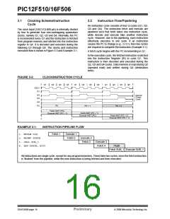
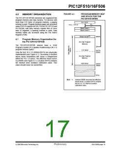
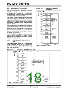
PIC12F510/16F506
For example, CLRF STATUS, will clear the upper three
bits and set the Z bit. This leaves the STATUS register
as 000u u1uu(where u= unchanged).
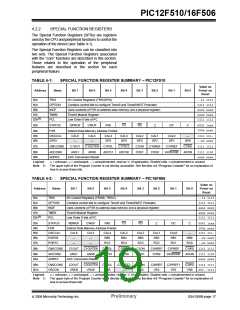
4.3
STATUS Register
This register contains the arithmetic status of the ALU,
the Reset status and the page preselect bit.
Therefore, it is recommended that only BCF, BSFand
MOVWFinstructions be used to alter the STATUS regis-
ter. These instructions do not affect the Z, DC or C bits
from the STATUS register. For other instructions which
do affect Status bits, see Section 11.0 “Instruction
Set Summary”.
The STATUS register can be the destination for any
instruction, as with any other register. If the STATUS
register is the destination for an instruction that affects
the Z, DC or C bits, then the write to these three bits is
disabled. These bits are set or cleared according to the
device logic. Furthermore, the TO and PD bits are not
writable. Therefore, the result of an instruction with the
STATUS register as destination may be different than
intended.
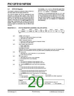
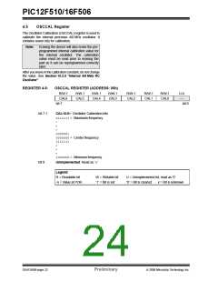
REGISTER 4-1:
STATUS REGISTER (ADDRESS: 03h) (PIC12F510)
R/W-0
R/W-0
CWUF
R/W-0
PA0
R-1
TO
R-1
PD
R/W-X
Z
R/W-X
DC
R/W-X
C
GPWUF
bit 7
bit 0
bit 7
bit 6
bit 5
GPWUF: GPIO Reset bit
1= Reset due to wake-up from Sleep on pin change
0= After power-up or other Reset
CWUF: Comparator Reset bit
1= Reset due to wake-up from Sleep on comparator change
0= After power-up or other Reset
PA0: Program Page Preselect bit
1= Page 1 (200h-3FFh)
0= Page 0 (000h-1FFh)
Each page is 512 bytes.
Using the PA0 bit as a general purpose read/write bit in devices which do not use it for program page
preselect is not recommended, since this may affect upward compatibility with future products.
bit 4
bit 3
bit 2
bit 1
TO: Time-out bit
1= After power-up, CLRWDTinstruction, or SLEEPinstruction
0= A WDT time-out occurred
PD: Power-down bit
1= After power-up or by the CLRWDTinstruction
0= By execution of the SLEEPinstruction
Z: Zero bit
1= The result of an arithmetic or logic operation is zero
0= The result of an arithmetic or logic operation is not zero
DC: Digit carry/borrow bit (for ADDWFand SUBWFinstructions)
ADDWF:
1= A carry from the 4th low-order bit of the result occurred
0= A carry from the 4th low-order bit of the result did not occur
SUBWF:
1= A borrow from the 4th low-order bit of the result did not occur
0= A borrow from the 4th low-order bit of the result occurred
bit 0
C: Carry/borrow bit (for ADDWF, SUBWFand RRF, RLFinstructions)
ADDWF:
SUBWF:
RRF or RLF:
1= A carry occurred
0= A carry did not occur
1= A borrow did not occur
0= A borrow occurred
Load bit with LSb or MSb, respectively
Legend:
R = Readable bit
-n = Value at POR
W = Writable bit
‘1’ = Bit is set
U = Unimplemented bit, read as ‘0’
‘0’ = Bit is cleared
x = Bit is unknown
DS41268B-page 18
Preliminary
© 2006 Microchip Technology Inc.

 ETC [ ETC ]