PIC12F510/16F506
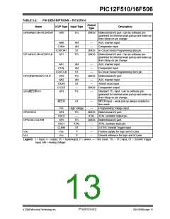
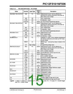
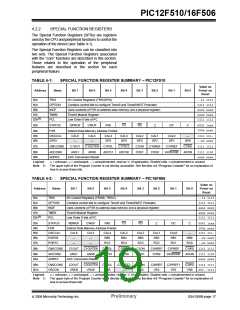
TABLE 3-3:
Name
PIN DESCRIPTIONS – PIC16F506
Output
Type
Function Input Type
Description
RB0/AN0/C1IN+/ICSPDAT
RB0
TTL
CMOS Bidirectional I/O port. Can be software pro-
grammed for internal weak pull-up and wake-up
from Sleep on pin change.
AN0
C1IN+
ICSPDAT
RB1
AN
AN
ST
—
—
ADC channel input.
Comparator 1 input.
CMOS In-Circuit Serial Programming data pin.
RB1/AN1/C1IN-/ICSPCLK
TTL
CMOS Bidirectional I/O port. Can be software pro-
grammed for internal weak pull-up and wake-up
from Sleep on pin change.
AN1
C1IN-
ICSPCLK
RB2
AN
AN
ST
—
—
—
ADC channel input.
Comparator 1 input.
In-Circuit Serial Programming clock pin.
RB2/AN2/C1OUT
RB3/MCLR/VPP
TTL
AN
—
CMOS Bidirectional I/O port.
ADC channel input.
CMOS Comparator 1 output.
AN2
—
C1OUT
RB3
TTL
—
Standard TTL input. Can be software programmed
for internal weak pull-up and wake-up from Sleep
on pin change.
MCLR
ST
—
—
MCLR input – weak pull-up always enabled in this
mode.
VPP
High Voltage
TTL
Programming voltage input.
RB4/OSC2/CLKOUT
RB5/OSC1/CLKIN
RB4
CMOS Bidirectional I/O port. Can be software pro-
grammed for internal weak pull-up and wake-up
from Sleep on pin change.
OSC2
CLKOUT
RB5
—
—
XTAL XTAL oscillator output pin.
CMOS EXTRC/INTOSC CLKOUT pin (FOSC/4).
CMOS Bidirectional I/O port.
TTL
XTAL
ST
OSC1
CLKIN
RC0
—
—
XTAL oscillator input pin.
EXTRC/EC Schmitt Trigger input.
RC0/C2IN+
RC1/C2IN-
RC2/CVREF
TTL
AN
TTL
AN
TTL
—
CMOS Bidirectional I/O port.
Comparator 2 input.
CMOS Bidirectional I/O port.
Comparator 2 input.
CMOS Bidirectional I/O port.
C2IN+
RC1
—
C2IN-
RC2
—
CVREF
RC3
AN
Programmable Voltage Reference output.
RC3
TTL
TTL
—
CMOS Bidirectional I/O port.
CMOS Bidirectional I/O port.
CMOS Comparator 2 output.
CMOS Bidirectional I/O port.
RC4/C2OUT
RC4
C2OUT
RC5
RC5/T0CKI
TTL
ST
T0CKI
VDD
—
—
—
Timer0 clock input.
VDD
VSS
P
Positive supply for logic and I/O pins.
Ground reference for logic and I/O pins.
VSS
P
Legend: I = input, O = output, I/O = input/output, P = power, — = Not Used, TTL = TTL input, ST = Schmitt Trigger
input, AN = Analog Voltage
© 2006 Microchip Technology Inc.
Preliminary
DS41268B-page 13

 ETC [ ETC ]