a-Si TFT LCD Single Chip Driver
240RGBx320 Resolution and 262K color
ILI9325
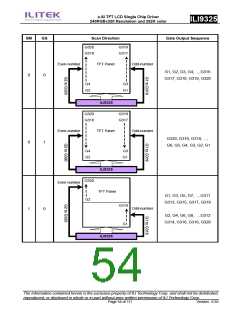
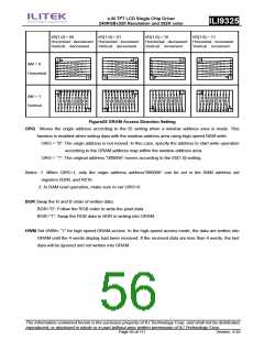
I/D[1:0] = 00
I/D[1:0] = 01
I/D[1:0] = 10
I/D[1:0] = 11
Horizontal : decrement Horizontal : increment
Horizontal : decrement Horizontal : increment
Vertical : decrement
Vertical : decrement
Vertical : increment
Vertical : increment
E
E
B
B
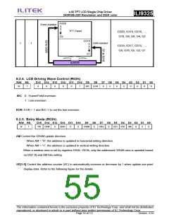
AM = 0
Horizontal
B
B
E
E
E
E
B
B
AM = 1
Vertical
B
B
E
E
Figure25 GRAM Access Direction Setting
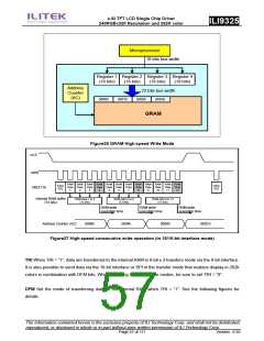
ORG Moves the origin address according to the ID setting when a window address area is made. This
function is enabled when writing data with the window address area using high-speed RAM write.
ORG = “0”: The origin address is not moved. In this case, specify the address to start write operation
according to the GRAM address map within the window address area.
ORG = “1”: The original address “00000h” moves according to the I/D[1:0] setting.
Notes: 1. When ORG=1, only the origin address address”00000h” can be set in the RAM address set
registers R20h, and R21h.
2. In RAM read operation, make sure to set ORG=0.
BGR Swap the R and B order of written data.
BGR=”0”: Follow the RGB order to write the pixel data.
BGR=”1”: Swap the RGB data to BGR in writing into GRAM.
HWM Set HWM= “1” for high speed GRAM access. In the high-speed access mode, the data are written into
GRAM until the 4 words display had been received. If the received data are less than 4 words, the last
data will be ignored and not written into GRAM.
The information contained herein is the exclusive property of ILI Technology Corp. and shall not be distributed,
reproduced, or disclosed in whole or in part without prior written permission of ILI Technology Corp.
Page 56 of 111
Version: 0.35

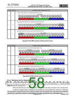
 ETC [ ETC ]