a-Si TFT LCD Single Chip Driver
240RGBx320 Resolution and 262K color
ILI9325
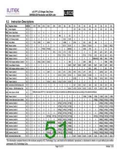
8.2.1. Index (IR)
R/W RS
D15 D14 D13 D12 D11 D10 D9 D8 D7 D6 D5 D4 D3 D2 D1 D0
W
0
-
-
-
-
-
-
-
-
ID7 ID6 ID5 ID4 ID3 ID2 ID1 ID0
The index register specifies the address of register (R00h ~ RFFh) or RAM which will be accessed.
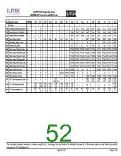
8.2.2. Start Oscillation (R00h)
R/W RS
D15 D14 D13 D12 D11 D10 D9 D8 D7 D6 D5 D4 D3 D2 D1 D0
W
R
1
1
-
-
-
-
-
-
-
-
-
-
-
-
-
-
-
1
1
1
0
0
1
0
0
1
1
0
0
1
0
0
1
0
The device code “9325”h is read out when read this register.
8.2.3. Driver Output Control (R01h)
R/W RS
D15 D14 D13 D12 D11 D10 D9 D8 D7 D6 D5 D4 D3 D2 D1 D0
W
1
0
0
0
0
0
SM SS
0
0
0
0
0
0
0
0
0
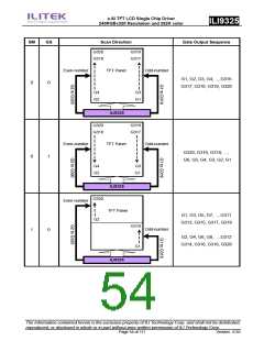
SS: Select the shift direction of outputs from the source driver.
When SS = 0, the shift direction of outputs is from S1 to S720
When SS = 1, the shift direction of outputs is from S720 to S1.
In addition to the shift direction, the settings for both SS and BGR bits are required to change the
assignment of R, G, B dots to the source driver pins.
To assign R, G, B dots to the source driver pins from S1 to S720, set SS = 0.
To assign R, G, B dots to the source driver pins from S720 to S1, set SS = 1.
When changing SS or BGR bits, RAM data must be rewritten.
SM: Sets the gate driver pin arrangement in combination with the GS bit (R60h) to select the optimal scan
mode for the module.
The information contained herein is the exclusive property of ILI Technology Corp. and shall not be distributed,
reproduced, or disclosed in whole or in part without prior written permission of ILI Technology Corp.
Page 53 of 111
Version: 0.35

 ETC [ ETC ]