a-Si TFT LCD Single Chip Driver
240RGBx320 Resolution and 262K color
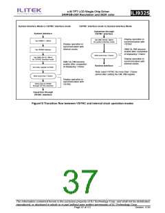
ILI9325
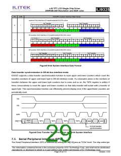
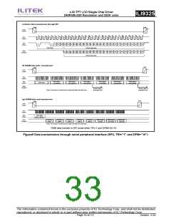
(e) Basic data transmission through SPI
Start
End
nCS
(Input)
1
0
2
1
3
1
4
1
5
0
6
7
8
9
10 11 12 13 14 15 16 17 18 19 20 21 22 23
25 26 27 28 29 30 31
24
32
SCL
(Input)
SDI
(Input)
D15 D14 D13 D12 D11 D10 D9 D8 D7 D6 D5 D4 D3 D2 D1 D0
D23 D22 D21 D120 D19 D18 D17 D16
D23 D22 D21 D120 D19 D18 D17 D16
ID RS RW
Start Byte
GRAM data write
SDO
(Output)
D15 D14 D13 D12 D11 D10 D9 D8 D7 D6 D5 D4 D3 D2 D1 D0
GRAM data read
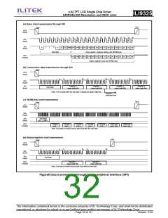
(f) GRAM data write transmission
End
Start
nCS
(Input)
SCL
(Input)
SDI
RAM data 1
1st transfer
RAM data 1
2nd transfer
RAM data 1
3rd transfer
RAM data 2
1st transfer
RAM data 2
2nd transfer
RAM data 2
3rd transfer
Start Byte
(Input)
SDO
(Output)
GRAM Data (1)
execution time
GRAM Data (2)
execution time
Note: Five bytes of invalid dummy data read after the start byte.
(g) GRAM data read transmission
End
Start
nCS
(Input)
SCL
(Input)
SDI
(Input)
Start Byte
RS=1, RW=1
SDO
(Output)
Dummy
read 1
Dummy
read 2
Dummy
read 3
Dummy
read 4
Dummy
read 5
RAM read
1st byte
RAM read
2nd byte
RAM read
3rd byte
Note: Five bytes of invalid dummy data read after the start byte.
RAM data transfer in SPI mode when TRI=1 and DFM[1:0]=10.
Figure9 Data transmission through serial peripheral interface (SPI), TRI=”1” and DFM=”10”)
The information contained herein is the exclusive property of ILI Technology Corp. and shall not be distributed,
reproduced, or disclosed in whole or in part without prior written permission of ILI Technology Corp.
Page 33 of 111
Version: 0.35

 ETC [ ETC ]