a-Si TFT LCD Single Chip Driver
240RGBx320 Resolution and 262K color
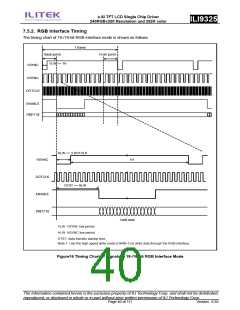
ILI9325
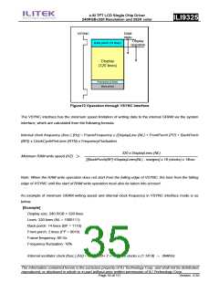
When calculate the internal clock frequency, the oscillator variation is needed to be taken into consideration.
In the above example, the calculated internal clock frequency with ±10% margin variation is considered and
ensures to complete the display operation within one VSYNC cycle. The causes of frequency variation come
from fabrication process of LSI, room temperature, external resistors and VCI voltage variation.
Minimum speed for RAM writing [Hz] > 240 x 320 x 394K / [ (14 + 320 – 2)lines x 16clocks] ≒ 5.7 MHz
The above theoretical value is calculated based on the premise that the ILI9325 starts to write data into the
internal GRAM on the falling edge of VSYNC. There must at least be a margin of 2 lines between the physical
display line and the GRAM line address where data writing operation is performed. The GRAM write speed of
5.7MHz or more will guarantee the completion of GRAM write operation before the ILI9325 starts to display
the GRAM data on the screen and enable to rewrite the entire screen without flicker.
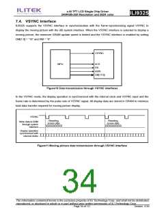
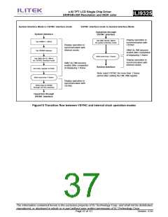
Notes in using the VSYNC interface
1. The minimum GRAM write speed must be satisfied and the frequency variation must be taken into
consideration.
2. The display frame rate is determined by the VSYNC signal and the period of VSYNC must be longer than
the scan period of an entire display.
3. When switching from the internal clock operation mode (DM[1:0] = “00”) to the VSYNC interface mode or
inversely, the switching starts from the next VSYNC cycle, i.e. after completing the display of the frame.
4. The partial display, vertical scroll, and interlaced scan functions are not available in VSYNC interface mode
and set the AM bit to “0” to transfer display data.
The information contained herein is the exclusive property of ILI Technology Corp. and shall not be distributed,
reproduced, or disclosed in whole or in part without prior written permission of ILI Technology Corp.
Page 36 of 111
Version: 0.35

 ETC [ ETC ]