a-Si TFT LCD Single Chip Driver
240RGBx320 Resolution and 262K color
ILI9325
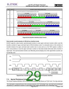
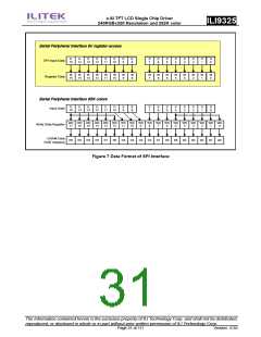
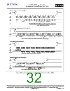
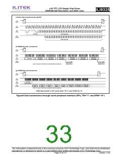
(nCS), the serial transfer clock pin (SCL), the serial data input pin (SDI) and the serial data output pin (SDO)
are used in SPI mode. The ID pin sets the least significant bit of the identification code. The DB[17:0] pins,
which are not used, must be tied to GND.
The SPI interface operation enables from the falling edge of nCS and ends of data transfer on the rising edge
of nCS. The start byte is transferred to start the SPI interface and the read/write operation and RS information
are also included in the start byte. When the start byte is matched, the subsequent data is received by
ILI9325.
The seventh bit of start byte is RS bit. When RS = “0”, either index write operation or status read operation is
executed. When RS = “1”, either register write operation or RAM read/write operation is executed. The eighth
bit of the start byte is used to select either read or write operation (R/W bit). Data is written when the R/W bit is
“0” and read back when the R/W bit is “1”.
After receiving the start byte, ILI9325 starts to transfer or receive the data in unit of byte and the data transfer
starts from the MSB bit. All the registers of the ILI9325 are 16-bit format and receive the first and the second
byte datat as the upper and the lower eight bits of the 16-bit register respectively. In SPI mode, 5 bytes
dummy read is necessary and the valid data starts from 6th byte of read back data.
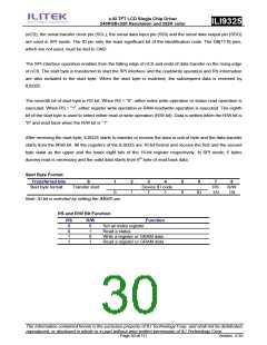
Start Byte Format
Transferred bits
S
1
2
3
4
5
6
7
8
Start byte format
Transfer start
Device ID code
RS
1/0
R/W
1/0
0
1
1
1
0
ID
Note: ID bit is selected by setting the IM0/ID pin.
RS and R/W Bit Function
RS
0
0
1
1
R/W
Function
0
1
0
1
Set an index register
Read a status
Write a register or GRAM data
Read a register or GRAM data
The information contained herein is the exclusive property of ILI Technology Corp. and shall not be distributed,
reproduced, or disclosed in whole or in part without prior written permission of ILI Technology Corp.
Page 30 of 111
Version: 0.35

 ETC [ ETC ]