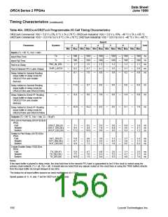
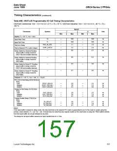
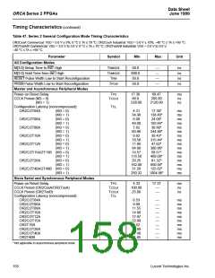
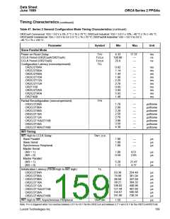
Data Sheet
June 1999
ORCA Series 2 FPGAs
Timing Characteristics (continued)
Table 46A. OR2CxxA/OR2TxxA Programmable I/O Cell Timing Characteristics
OR2CxxA Commercial: VDD = 5.0 V ± 5%, 0 °C ≤ TA ≤ 70 °C; OR2CxxA Industrial: VDD = 5.0 V ± 10%, –40 °C ≤ TA ≤ +85 °C.
OR2TxxA Commercial: VDD = 3.0 V to 3.6 V, 0 °C ≤ TA ≤ 70 °C; OR2TxxA Industrial: VDD = 3.0 V to 3.6 V, –40 °C ≤ TA ≤ +85 °C.
Speed
Parameter
Symbol
-2
-3
-4
-5
-6
-7
Unit
Min Max Min Max Min Max Min Max Min Max Min Max
Inputs (TJ = 85 °C, VDD = min)
Input Rise Time
TR
TF
—
—
—
—
—
500
500
1.7
6.2
8.1
—
—
—
—
—
500
500
1.5
4.7
7.0
—
—
—
—
—
500
500
1.3
4.1
6.0
—
—
—
—
—
500
500
1.2
3.5
5.9
—
—
—
—
—
500
500
1.2
3.1
6.2
—
—
—
—
—
500
500
1.1
2.9
5.8
ns
ns
ns
ns
ns
Input Fall Time
PAD_IN_DEL
CHIP_LATCH
—
Pad to In Delay
Pad to Nearest PFU Latch Output
Delay Added to General Routing
(input buffer in delay mode for
OR2C/2T15A and smaller
devices)
—
—
—
—
11.0
8.0
—
—
9.7
6.8
—
—
8.6
5.9
—
—
8.6
6.0
—
—
9.0
6.4
—
—
8.6
6.0
ns
ns
Delay Added to General Routing
(input buffer in delay mode for
OR2C/2T26A and OR2C/2T40A)
Delay Added to Direct-FF Routing
(input buffer in delay mode for
OR2C/2T15A and smaller
devices)
—
—
10.9
—
10.2
—
8.5
—
8.6
—
9.1
—
7.9
ns
Delay Added to Direct-FF Routing
(input buffer in delay mode for
OR2C/2T26A and OR2C/2T40A)
Outputs (TJ = 85 °C, VDD = min, CL = 50 pF)
PFU CK to Pad Delay (DOUT[3:0] to
PAD):
Fast
Slewlim
Sinklim
DOUT_DEL(F)
DOUT_DEL(SL)
DOUT_DEL(SI)
—
—
—
7.1
9.4
11.2
—
—
—
6.2
8.4
10.5
—
—
—
5.5
7.4
9.4
—
—
—
5.0
6.4
9.5
—
—
—
4.4
5.6
8.3
—
—
—
3.3
4.1
7.2
ns
ns
ns
Output to Pad Delay (OUT[3:0] to
PAD):
Fast
Slewlim
Sinklim
OUT_DEL(F)
OUT_DEL(SL)
OUT_DEL(SI)
—
—
—
5.0
6.7
9.8
—
—
—
4.0
6.3
7.2
—
—
—
3.6
5.5
7.5
—
—
—
3.1
4.5
7.6
—
—
—
2.7
3.9
6.5
—
—
—
2.3
3.1
6.2
ns
ns
ns
3-state Enable Delay (TS[3:0] to
PAD):
Fast
Slewlim
Sinklim
TS_DEL(F)
TS_DEL(SL)
TS_DEL(SI)
—
—
—
5.8
7.5
10.6
—
—
—
4.7
7.0
7.9
—
—
—
4.0
6.3
8.4
—
—
—
3.5
5.2
9.3
—
—
—
3.1
4.7
8.0
—
—
—
2.5
3.7
7.6
ns
ns
ns
Notes:
If the input buffer is placed in delay mode, the chip hold time to the nearest PFU latch is guaranteed to be 0 if the clock is routed using the
primary clock network; (TJ = all, VDD = all). It should also be noted that any signals routed on the clock lines or using the TRIDI buffers directly
from the input buffer do not get delayed at any time.
The delays for all input buffers assume an input rise/fall time of ≤1 V/ns.
Speed grades of -5, -6, and -7 are for OR2TxxA devices only
156
Lucent Technologies Inc.

 ETC [ ETC ]