Data Sheet
June 1999
ORCA Series 2 FPGAs
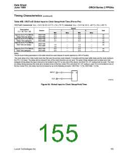
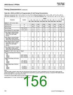
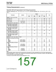
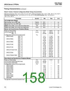
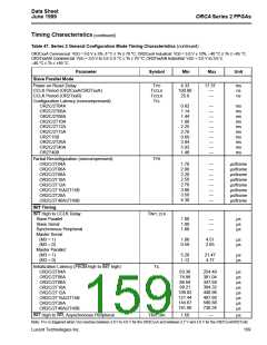
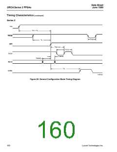
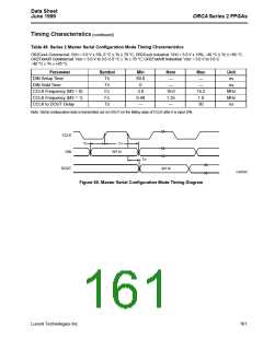
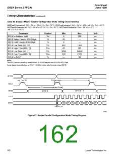
Timing Characteristics (continued)
Table 47. Series 2 General Configuration Mode Timing Characteristics (continued)
OR2CxxA Commercial: VDD = 5.0 V ± 5%, 0 °C ≤ TA ≤ 70 °C; OR2CxxA Industrial: VDD = 5.0 V ± 10%, –40 °C ≤ TA ≤ +85 °C.
OR2TxxA/B Commercial: VDD = 3.0 V to 3.6 V, 0 °C ≤ TA ≤ 70 °C; OR2TxxA/B Industrial: VDD = 3.0 V to 3.6 V,
–40 °C ≤ TA ≤ +85 °C.
Parameter
Symbol
Min
Max
Unit
Slave Parallel Mode
Power-on Reset Delay
TPO
TCCLK
TCCLK
TCL
4.33
100.00
25.0
17.37
—
ms
ns
ns
CCLK Period (OR2CxxA/OR2TxxA)
CCLK Period (OR2TxxB)
Configuration Latency (noncompressed):
OR2C/2T04A
—
0.82
1.14
1.44
1.86
2.25
2.76
0.69
3.84
5.93
1.48
—
—
—
—
—
—
—
—
—
—
ms
ms
ms
ms
ms
ms
ms
ms
ms
ms
OR2C/2T06A
OR2C/2T08A
OR2C/2T10A
OR2C/2T12A
OR2C/2T15A
OR2T15B
OR2C/2T26A
OR2C/2T40A
OR2T40B
Partial Reconfiguration (noncompressed):
OR2C/2T04A
TPR
1.70
2.00
2.20
2.50
2.70
3.00
3.50
4.30
—
—
—
—
—
—
—
—
µs/frame
µs/frame
µs/frame
µs/frame
µs/frame
µs/frame
µs/frame
µs/frame
OR2C/2T06A
OR2C/2T08A
OR2C/2T10A
OR2C/2T12A
OR2C/2T15A/2T15B
OR2C/2T26A
OR2C/2T40A/2T40B
INIT Timing
INIT High to CCLK Delay:
Slave Parallel
Slave Serial
Synchronous Peripheral
Master Serial:
(M3 = 1)
TINIT_CLK
1.00
1.00
1.00
—
—
—
µs
µs
µs
1.06
0.59
4.51
2.65
µs
µs
(M3 = 0)
Master Parallel:
(M3 = 1)
(M3 = 0)
5.28
1.12
21.47
4.77
µs
µs
Initialization Latency (PRGM high to INIT high):
OR2C/2T04A
TIL
63.36
74.98
86.59
254.40
301.04
347.68
394.32
440.96
487.60
580.88
730.34
µs
µs
µs
µs
µs
µs
µs
µs
OR2C/2T06A
OR2C/2T08A
OR2C/2T10A
OR2C/2T12A
OR2C/2T15A/2T15B
OR2C/2T26A
OR2C/2T40A/2T40B
98.21
109.82
121.44
144.67
181.90
INIT High to WR, Asynchronous Peripheral
TINIT_WR
1.50
—
µs
Note: TPO is triggered when VDD reaches between 3.0 V to 4.0 V for the OR2CxxA and between 2.7 V and 3.0 V for the OR2TxxA/OR2TxxB.
Lucent Technologies Inc.
159

 ETC [ ETC ]