Data Sheet
June 1999
ORCA Series 2 FPGAs
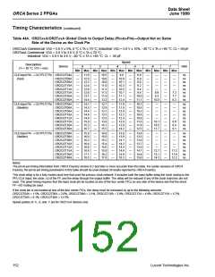
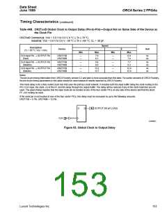
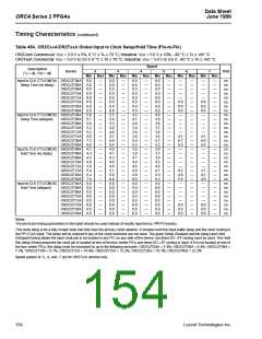
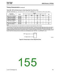
Timing Characteristics (continued)
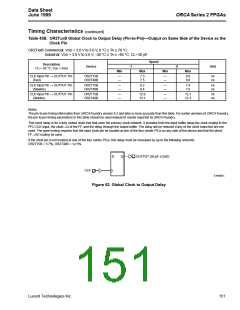
Table 44A. OR2CxxA/OR2TxxA Global Clock to Output Delay (Pin-to-Pin)—Output Not on Same
Side of the Device as the Clock Pin
OR2CxxA Commercial: VDD = 5.0 V ± 5%, 0 °C ≤ TA ≤ 70 °C; Industrial: VDD = 5.0 V ± 10%, –40 °C ≤ TA ≤ +85 °C; CL = 50 pF.
OR2TxxA Commercial: VDD = 3.0 V to 3.6 V, 0 °C ≤ TA ≤ 70 °C;
Industrial: VDD = 3.0 V to 3.6 V, –40 °C ≤ TA ≤ +85 °C; CL = 50 pF.
Speed
Description
(TJ = 85 °C, VDD = min)
Device
-2
-3
-4
-5
-6
-7
Unit
Min Max Min Max Min Max Min Max Min Max Min Max
CLK Input Pin → OUTPUT Pin OR2C/2T04A
—
—
—
—
—
—
—
—
11.8
12.0
12.2
12.4
12.6
12.8
13.1
14.4
—
—
—
—
—
—
—
—
10.5
10.6
10.8
11.0
11.2
11.5
11.9
13.3
—
—
—
—
—
—
—
—
9.9
—
—
—
—
—
—
—
—
8.8
8.9
9.0
9.2
9.4
9.6
10.0
11.1
—
—
—
—
—
—
—
—
—
—
—
—
—
8.9
9.3
10.5
—
—
—
—
—
—
—
—
—
—
—
—
—
7.3
7.7
8.3
ns
ns
ns
ns
ns
ns
ns
ns
(Fast)
OR2C/2T06A
OR2C/2T08A
OR2C/2T10A
OR2C/2T12A
OR2C/2T15A
OR2C/2T26A
OR2C/2T40A
10.0
10.1
10.3
10.5
10.7
11.1
12.4
CLK Input Pin → OUTPUT Pin OR2C/2T04A
—
—
—
—
—
—
—
—
14.1
14.3
14.4
14.6
14.8
15.0
15.3
16.7
—
—
—
—
—
—
—
—
12.7
12.9
13.1
13.3
13.5
13.6
14.1
15.5
—
—
—
—
—
—
—
—
11.8
11.9
12.0
12.2
12.4
12.6
12.9
14.2
—
—
—
—
—
—
—
—
10.3
10.4
10.5
10.6
10.8
11.0
11.4
12.5
—
—
—
—
—
—
—
—
—
—
—
—
—
10.1
10.5
11.7
—
—
—
—
—
—
—
—
—
—
—
—
—
8.0
8.4
9.1
ns
ns
ns
ns
ns
ns
ns
ns
(Slewlim)
OR2C/2T06A
OR2C/2T08A
OR2C/2T10A
OR2C/2T12A
OR2C/2T15A
OR2C/2T26A
OR2C/2T40A
CLK Input Pin → OUTPUT Pin OR2C/2T04A
—
—
—
—
—
—
—
—
15.9
16.0
16.2
16.4
16.6
16.8
17.1
18.5
—
—
—
—
—
—
—
—
14.8
15.0
15.2
15.4
15.6
15.8
16.2
17.6
—
—
—
—
—
—
—
—
13.8
13.9
14.1
14.2
14.4
14.6
14.9
16.3
—
—
—
—
—
—
—
—
13.4
13.5
13.6
13.7
13.9
14.1
14.4
15.6
—
—
—
—
—
—
—
—
—
—
—
—
—
12.7
13.1
14.3
—
—
—
—
—
—
—
—
—
—
—
—
—
11.2
11.6
12.2
ns
ns
ns
ns
ns
ns
ns
ns
(Sinklim)
OR2C/2T06A
OR2C/2T08A
OR2C/2T10A
OR2C/2T12A
OR2C/2T15A
OR2C/2T26A
OR2C/2T40A
Notes:
The pin-to-pin timing information from ORCA Foundry version 9.2 and later is more accurate than this table. For earlier versions of ORCA
Foundry, the pin-to-pin timing parameters in this table should be used instead of results reported by ORCA Foundry.
This clock delay is for a fully routed clock tree that uses the primary clock network. It includes both the input buffer delay,the clock routing to the
PFU CLK input, the clock→Q of the FF, and the delay through the output buffer. The delay will be reduced if any of the clock branches are not
used. The given timing requires that the input clock pin be located at one of the four center PICs on any side of the device and that the direct
FF→I/O routing be used.
If the clock pin is not located at one of the four center PICs, this delay must be increased by up to the following amounts:
OR2C/2T04A = 1.5%, OR2C/2T06A = 2.0%, OR2C/2T08A = 3.1%, OR2C/2T10A = 3.9%, OR2C/2T12A = 4.9%, OR2C/2T15A = 5.7%,
OR2C/2T26A = 8.1%, OR2C/2T40A = 12.5%.
Speed grades of -5, -6, and -7 are for OR2TxxA devices only
152
Lucent Technologies Inc.

 ETC [ ETC ]