Data Sheet
June 1999
ORCA Series 2 FPGAs
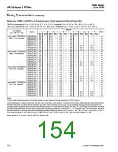
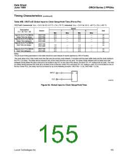
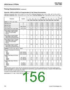
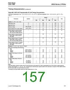
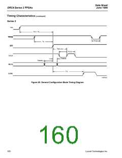
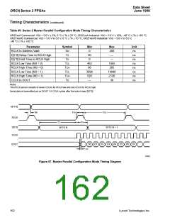
Timing Characteristics (continued)
Table 47. Series 2 General Configuration Mode Timing Characteristics
OR2CxxA Commercial: VDD = 5.0 V ± 5%, 0 °C ≤ TA ≤ 70 °C; OR2CxxA Industrial: VDD = 5.0 V ± 10%, –40 °C ≤ TA ≤ +85 °C.
OR2TxxA/B Commercial: VDD = 3.0 V to 3.6 V, 0 °C ≤ TA ≤ 70 °C; OR2TxxA/B Industrial: VDD = 3.0 V to 3.6 V,
–40 °C ≤ TA ≤ +85 °C.
Parameter
All Configuration Modes
Symbol
Min
Max
Unit
M[3:0] Setup Time to INIT High
TSMODE
THMODE
TRW
50.0
600.0
50.0
—
—
—
—
ns
ns
ns
ns
M[3:0] Hold Time from INIT High
RESET Pulse Width Low to Start Reconfiguration
PRGM Pulse Width Low to Start Reconfiguration
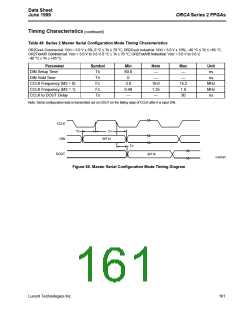
Master and Asynchronous Peripheral Modes
TPGW
50.0
Power-on Reset Delay
CCLK Period (M3 = 0)
(M3 = 1)
TPO
TCCLK
17.30
66.0
528.00
69.47
265.00
2120.00
ms
ns
ns
Configuration Latency (noncompressed):
TCL
OR2C/2T04A
OR2C/2T06A
OR2C/2T08A
OR2C/2T10A
OR2C/2T12A
(M3 = 0)
(M3 = 1)
(M3 = 0)
(M3 = 1)
(M3 = 0)
(M3 = 1)
(M3 = 0)
(M3 = 1)
(M3 = 0)
(M3 = 1)
4.31
34.48
6.00
48.00
7.62
17.30*
138.40*
24.08*
192.64*
30.60*
244.80*
39.43*
315.44*
47.62*
380.96*
58.51*
468.08*
81.32*
650.56*
125.62*
1004.96*
ms
ms
ms
ms
ms
ms
ms
ms
ms
ms
ms
ms
ms
ms
ms
ms
60.96
9.82
78.56
11.86
94.88
14.57
116.56
20.25
162.00
31.29
250.32
OR2C/2T15A/2T15B (M3 = 0)
(M3 = 1)
OR2C/2T26A
(M3 = 0)
(M3 = 1)
OR2C/2T40A/2T40B (M3 = 0)
(M3 = 1)
Slave Serial and Synchronous Peripheral Modes
Power-on Reset Delay
CCLK Period (OR2CxxA/OR2TxxA)
CCLK Period (OR2TxxB)
Configuration Latency (noncompressed):
OR2C/2T04A
TPO
TCCLK
TCCLK
TCL
4.33
100.00
25.00
17.37
—
—
ms
ns
ns
6.53
9.09
—
—
—
—
—
—
—
—
—
—
ms
ms
ms
ms
ms
ms
ms
ms
ms
ms
OR2C/2T06A
OR2C/2T08A
OR2C/2T10A
OR2C/2T12A
OR2C/2T15A
OR2T15B
OR2C/2T26A
OR2C/2T40A
11.55
14.88
17.97
22.08
5.52
30.69
47.40
11.85
OR2T40B
* Not applicable to asynchronous peripheral mode.
158
Lucent Technologies Inc.

 ETC [ ETC ]