HY29F800
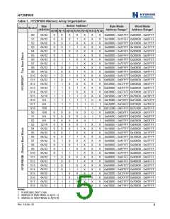
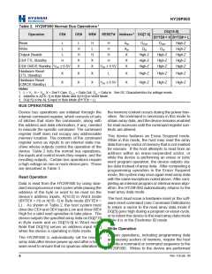
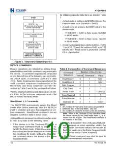
Table 2. HY29F800 Normal Bus Operations1
DQ[15:8]
BYTE# = H BYTE# = L
Operation
CE#
OE#
WE#
RESET# Address 2 DQ[7:0]
Read
Write
L
L
L
H
H
X
X
H
L
H
AIN
AIN
X
DOUT
DIN
DOUT
DIN
High-Z
High-Z
High-Z
High-Z
High-Z
H
Output Disable
L
H
X
X
H
H
High-Z
High-Z
High-Z
High-Z
High-Z
High-Z
CE# TTL Standby
H
X
CE# CMOS Standby VCC ± 0.5V
VCC ± 0.5V
X
Hardware Reset
X
X
X
X
X
L
X
X
High-Z
High-Z
High-Z
High-Z
High-Z
High-Z
(TTL Standby)
Hardware Reset
X
VSS ± 0.5V
(CMOS Standby)
Notes:
1. L = VIL, H = VIH, X = Don’t Care, DOUT = Data Out, DIN = Data In. See DC Characteristics for voltage levels.
2. Address is A[18:-1] in Byte Mode and A[18:0] in Word Mode.
3. DQ[15] is the A[-1] input in Byte Mode (BYTE# = L).
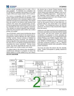
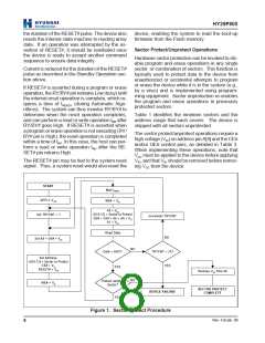
BUS OPERATIONS
Device bus operations are initiated through the
internal command register, which consists of sets
of latches that store the commands, along with
the address and data information, if any, needed
to execute the specific command. The command
register itself does not occupy any addressable
memory location. The contents of the command
register serve as inputs to an internal state ma-
chine whose outputs control the operation of the
device. Table 2 lists the normal bus operations,
the inputs and control levels they require, and the
resulting outputs. Certain bus operations require
a high voltage on one or more device pins. Those
are described in Table 3.
the memory content occurs during the power tran-
sition. No command is necessary in this mode to
obtain array data, and the device remains enabled
for read accesses until the command register con-
tents are altered.
This device features an Erase Suspend mode.
While in this mode, the host may read the array
data from any sector of memory that is not marked
for erasure. If the host attempts to read from an
address within an erase-suspended sector, or
while the device is performing an erase or byte/
word program operation, the device outputs sta-
tus data instead of array data. After completing a
programming operation in the Erase Suspend
mode, the system may once again read array data
with the same exceptions noted above. After com-
pleting an internal program or internal erase algo-
rithm, the HY29F800 automatically returns to the
read array data mode.
Read Operation
Data is read from the HY29F800 by using stan-
dard microprocessor read cycles while placing the
address of the byte or word to be read on the
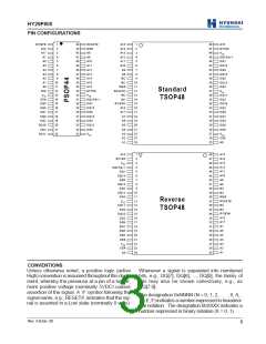
device’s address inputs, A[18:0] in Word mode
(BYTE# = H) or A[18:-1] in Byte mode (BYTE# =
L) . As shown in Table 2, the host system must
drive the CE# and OE# inputs Low and drive WE#
High for a valid read operation to take place. The
device outputs the specified array data on DQ[7:0]
in Byte mode and on DQ[15:0] in Word mode.
Note that DQ[15] serves as address input A[-1]
when the device is operating in Byte mode.
The host must issue a hardware reset or the soft-
ware reset command (see Command Definitions)
to return a sector to the read array data mode if
DQ[5] goes high during a program or erase cycle,
or to return the device to the read array data mode
while it is in the Electronic ID mode.
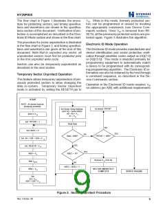
Write Operation
Certain operations, including programming data
and erasing sectors of memory, require the host
to write a command or command sequence to the
HY29F800. Writes to the device are performed
The HY29F800 is automatically set for reading
array data after device power-up and after a hard-
ware reset to ensure that no spurious alteration of
Rev. 4.0/Jan. 00
6

 ETC [ ETC ]