HY29F800
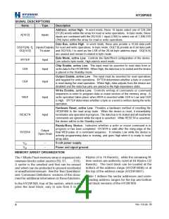
SIGNAL DESCRIPTIONS
Name
Type
Description
Address, active High. In word mode, these 19 inputs select one of 524,288
(512K) words within the array for read or write operations. In byte mode, these
inputs are combined with the DQ15/A-1 input (LSB) to select one of 1,048,576
(1M) bytes within the array for read or write operations.
A[18:0]
Inputs
Data Bus, active High. In word mode, these pins provide a 16-bit data path
DQ[15]/A[-1], Inputs/Outputs for read and write operations. In byte mode, DQ[7:0] provide an 8-bit data path
DQ[14:0]
BYTE#
CE#
Tri-state
and DQ15/A-1 is used as the LSB of the 20-bit byte address input. DQ[14:8]
are unused and remain tri-stated in byte mode.
Byte Mode, active Low. Controls the Byte/Word configuration of the device.
Low selects byte mode, High selects word mode.
Input
Chip Enable, active Low. This input must be asserted to read data from or
write data to the HY29F800. WhenHigh, the data bus is tri-stated and the device
is placed in the Standby mode.
Input
Output Enable, active Low. This input must be asserted for read operations
and negated for write operations. BYTE# determines whether a byte or a word
is read during the read operation. When High, data outputs from the device are
disabled and the data bus pins are placed in the high impedance state.
OE#
WE#
Input
Input
Write Enable, active Low. Controls writing of commands or command
sequences in order to program data or erase sectors of the memory array. A
write operation takes place when WE# is asserted while CE# is Low and OE#
is High. BYTE# determines whether a byte or a word is written during the write
operation.
Hardware Reset, active Low. Provides a hardware method of resetting the
HY29F800 to the read array state. When the device is reset, it immediately
terminates any operationinprogress. The data bus is tri-stated and all read/write
commands are ignored while the input is asserted. While RESET# is asserted,
the device will be in the Standby mode.
RESET#
RY/BY#
Input
Ready/Busy Status. Indicates whether a write or erase command is in
progress or has been completed. RY/BY# is valid after the rising edge of the
final WE# pulse of a command sequence. It remains Low while the device is
actively programming data or erasing, and goes High when it is ready to read
array data.
Output
Open Drain
5-volt power supply.
VCC
VSS
--
--
Power and signal ground.
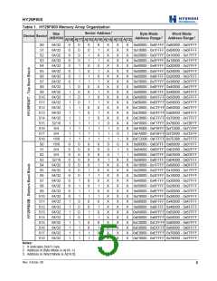
MEMORY ARRAY ORGANIZATION
Kbytes (4 to 16 Kwords), while the remaining fif-
teen sectors are uniformly sized at 64 Kbytes (32
Kwords). The boot block can be located at the
bottom of the address range (HY29F800B) or at
the top of the address range (HY29F800T).
The 1 Mbyte Flash memory array is organized into
nineteen blocks called sectors (S0, S1, . . . , S18).
A sector is the smallest unit that can be erased
and which can be protected to prevent accidental
or unauthorized erasure. See the ‘Bus Operations’
and ‘Command Definitions’ sections of this docu-
ment for additional information on these functions.
Table 1 defines the sector addresses and corre-
sponding address ranges for the top and bottom
boot block versions of the HY29F800.
In the HY29F800, four of the sectors, which com-
prise the boot block, vary in size from 8 to 32
Rev. 4.0/Jan. 00
4

 ETC [ ETC ]