HY29F800
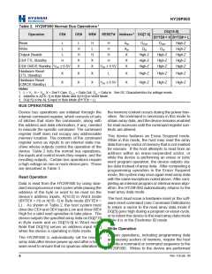
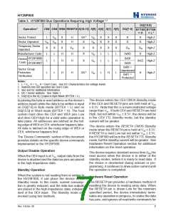
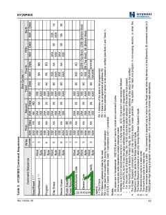
Table 3. HY29F800 Bus Operations Requiring High Voltage1, 2
DQ[15:8]
Operation3
CE# OE# WE# RESET# A[18:12] A[9] A[6] A[1] A[0] DQ[7:0]
BYTE# BYTE#
= H
= L5
Sector Protect
L
VID
X
X
H
H
SA4
X
VID
VID
X
X
X
X
X
X
X
X
X
High-Z
High-Z
Sector Unprotect
VID VID
X
Temporary Sector
Unprotect
X
L
X
L
X
H
VID
H
X
X
X
X
L
X
L
X
L
DIN
DIN
X
High-Z
High-Z
Manufacturer Code
VID
0xAD
0x58
0xD6
HY29F800B
HY29F800T
Device
Code
L
L
H
H
X
VID
L
L
H
0x22 High-Z
0x00 =
Unprotected
Sector Group
Protection
Verification
L
L
H
H
SA4
VID
L
H
L
X
High-Z
0x01 =
Protected
Notes:
1. L = VIL, H = VIH, X = Don’t Care. See DC Characteristics for voltage levels.
2. Address bits not specified are Don’t Care.
3. See text for additional information.
4. SA = sector address. See Table 1.
5. DQ[15] is the A[-1] input in Byte Mode (BYTE# = L).
The device enters the CE# CMOS Standby mode
if the CE# and RESET# pins are both held at VCC
± 0.5V. Note that this is a more restricted voltage
range than VIH. If both CE# and RESET# are held
High, but not within VCC ± 0.5V, the device will be
in the CE# TTL Standby mode, but the standby
current will be greater.
by placing the byte or word address on the device’s
address inputs while the data to be written is input
on DQ[7:0] in Byte mode (BYTE# = L) and on
DQ[15:0] in Word mode (BYTE# = H). The host
system must drive the CE# and WE# pins Low
and drive OE# High for a valid write operation to
take place. All addresses are latched on the fall-
ing edge of WE# or CE#, whichever happens later.
All data is latched on the rising edge of WE# or
CE#, whichever happens first.
The device enters the RESET# CMOS Standby
mode when the RESET# pin is held at VSS ± 0.5V.
If RESET# is held Low but not within VSS ± 0.5V,
the HY29F800 will be in the RESET# TTL Standby
mode, but the standby current will be greater. See
Hardware Reset Operation section for additional
information on the reset operation.
The ‘Device Commands’ section of this document
provides details on the specific device commands
implemented in the HY29F800.
Output Disable Operation
The device requires standard access time (tCE) for
read access when the device is in either of the
standby modes, before it is ready to read data. If
the device is deselected during erasure or pro-
gramming, it continues to draw active current until
the operation is completed.
When the OE# input is at VIH, output data from the
device is disabled and the data bus pins are placed
in the high impedance state.
Standby Operation
When the system is not reading from or writing to
the HY29F800, it can place the device in the
Standby mode. In this mode, current consump-
tion is greatly reduced, and the data bus outputs
are placed in the high impedance state, indepen-
dent of the OE# input. The Standby mode can
invoked using two methods.
Hardware Reset Operation
The RESET# pin provides a hardware method of
resetting the device to reading array data. When
the RESET# pin is driven Low for the minimum
specified period, the device immediately termi-
nates any operation in progress, tri-states the data
bus pins, and ignores all read/write commands for
Rev. 4.0/Jan. 00
7

 ETC [ ETC ]