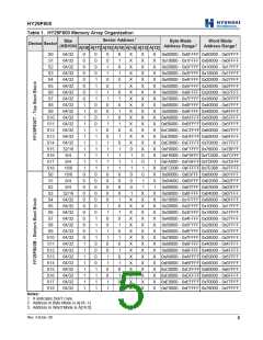
HY29F800
PIN CONFIGURATIONS
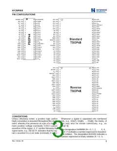
RY/BY#
A18
A17
A7
1
2
3
4
5
6
7
44
43
42
41
40
39
38
RESET#
WE#
A8
A15
A14
A13
A12
A11
A10
A9
1
2
3
4
5
6
7
48
47
46
45
44
43
42
A16
BYTE#
VSS
A9
DQ15/A-1
DQ7
A6
A10
A5
A11
DQ14
DQ6
A4
A12
A3
A2
8
9
37
36
A13
A14
A8
NC
8
9
41
40
DQ13
DQ5
A1
A0
10
11
35
34
A15
A16
NC
10
11
39
38
DQ12
DQ4
WE#
Standard
TSOP48
CE#
VSS
12
13
14
15
33
32
31
30
BYTE#
VSS
RESET#
NC
12
13
14
15
37
36
35
34
VCC
DQ11
DQ3
DQ10
OE#
DQ0
DQ15/A-1
DQ7
NC
RY/BY#
DQ8
DQ1
16
17
18
19
20
29
28
27
26
25
DQ14
DQ6
A18
A17
A7
16
17
18
19
20
33
32
31
30
29
DQ2
DQ9
DQ1
DQ8
DQ0
DQ9
DQ13
DQ5
DQ2
A6
DQ10
DQ12
A5
DQ3
21
22
24
23
DQ4
VCC
A4
A3
A2
A1
21
22
23
24
28
27
26
25
OE#
VSS
CE#
A0
DQ11
A15
A14
A13
A12
A11
A10
A9
A16
BYTE#
VSS
1
2
3
4
5
6
7
48
47
46
45
44
43
42
DQ15/A-1
DQ7
DQ14
DQ6
A8
NC
DQ13
DQ5
8
9
41
40
NC
DQ12
DQ4
10
11
39
38
WE#
RESET#
NC
Reverse
TSOP48
VCC
DQ11
DQ3
12
13
14
15
37
36
35
34
NC
RY/BY#
A18
A17
A7
DQ10
DQ2
DQ9
DQ1
DQ8
DQ0
16
17
18
19
20
33
32
31
30
29
A6
A5
A4
A3
A2
A1
OE#
VSS
CE#
A0
21
22
23
24
28
27
26
25
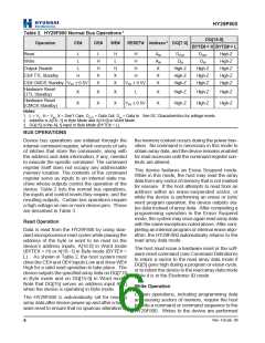
CONVENTIONS
Unless otherwise noted, a positive logic (active
High) convention is assumed throughout this docu-
ment, whereby the presence at a pin of a higher,
more positive voltage (nominally 5VDC) causes
assertion of the signal. A ‘#’ symbol following the
signal name, e.g., RESET#, indicates that the sig-
nal is asserted in a Low state (nominally 0 volts).
Whenever a signal is separated into numbered
bits, e.g., DQ[7], DQ[6], ..., DQ[0], the family of
bits may also be shown collectively, e.g., as
DQ[7:0].
The designation 0xNNNN (N = 0, 1, 2, . . . , 9, A, .
. . , E, F) indicates a number expressed in hexadeci-
mal notation. The designation 0bXXXX indicates a
number expressed in binary notation (X = 0, 1).
Rev. 4.0/Jan. 00
3

 ETC [ ETC ]