HY29F800
A 55ns version operating over 5.0 volts ± 5% is
also available. To eliminate bus contention, the
HY29F800 has separate chip enable (CE#), write
enable (WE#) and output enable (OE#) controls.
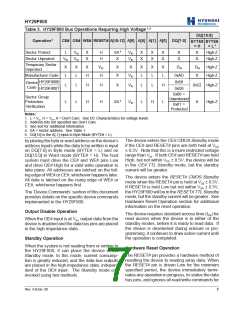
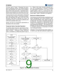
the device has a Sector Protect function which
hardware write protects selected sectors. The
sector protect and unprotect features can be en-
abled in a PROM programmer. Temporary Sec-
tor Unprotect, which requires a high voltage, al-
lows in-system erasure and code changes in pre-
viously protected sectors.
The device is compatible with the JEDEC single
power-supply Flash command set standard. Com-
mands are written to the command register using
standard microprocessor write timings, from where
they are routed to an internal state-machine that
controls the erase and programming circuits.
Device programming is performed a byte at a time
by executing the four-cycle Program Command.
This initiates an internal algorithm that automati-
cally times the program pulse widths and verifies
proper cell margin.
Erase Suspend enables the user to put erase on
hold for any period of time to read data from, or
program data to, any sector that is not selected
for erasure. True background erase can thus be
achieved. The device is fully erased when shipped
from the factory.
Addresses and data needed for the programming
and erase operations are internally latched during
write cycles, and the host system can detect
completion of a program or erase operation by
observing the RY/BY# pin, or by reading the DQ[7]
(Data# Polling) and DQ[6] (toggle) status bits.
Reading data from the device is similar to reading
from SRAM or EPROM devices. Hardware data
protection measures include a low VCC detector
that automatically inhibits write operations during
power transitions.
The HY29F800’s sector erase architecture allows
any number of array sectors to be erased and re-
programmed without affecting the data contents
of other sectors. Device erasure is initiated by
executing the Erase Command. This initiates an
internal algorithm that automatically preprograms
the array (if it is not already programmed) before
executing the erase operation. During erase
cycles, the device automatically times the erase
pulse widths and verifies proper cell margin.
The host can place the device into the standby
mode. Power consumption is greatly reduced in
this mode.
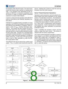
To protect data in the device from accidental or
unauthorized attempts to program or erase the
device while it is in the system (e.g., by a virus),
BLOCK DIAGRAM
DQ[15:0]
A[18:0], A-1
DQ[15:0]
STATE
CONTROL
ERASE VOLTAGE
GENERATOR AND
SECTOR SWITCHES
I/O BUFFERS
DATA LATCH
Y-GATING
COMMAND
REGISTER
WE#
CE#
I/O CONTROL
OE#
PROGRAM
VOLTAGE
GENERATOR
BYTE#
RESET#
RY/BY#
Y-DECODER
X-DECODER
A[18:0], A-1
8 Mb FLASH
MEMORY
ARRAY
VC C DETECTOR
TIMER
Rev. 4.0/Jan. 00
2

 ETC [ ETC ]