AD797
NO ISE AND SO URCE IMP ED ANCE CO NSID ERATIO NS
T he AD797’s ultralow voltage noise of 0.9 nV/√Hz is achieved
with special input transistors running at nearly 1 mA of collector
current. It is important then to consider the total input referred
noise (eNtotal), which includes contributions from voltage noise
(eN), current noise (iN), and resistor noise (√4 kTrS).
2
LO W FREQ UENCY NO ISE
Analog Devices specifies low frequency noise as a peak to peak
(p-p) quantity in a 0.1 Hz to 10 Hz bandwidth. Several tech-
niques can be used to make this measurement. T he usual tech-
nique involves amplifying, filtering, and measuring the amplifiers
noise for a predetermined test time. T he noise bandwidth of the
filter is corrected for and the test time is carefully controlled
since the measurement time acts as an additional low frequency
roll-off.
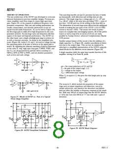
eNtotal = [eN + 4 kTrS + 4 (iNrS)2]l/2
Equation 1
where rS = total input source resistance.
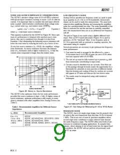
T his equation is plotted for the AD797 in Figure 30. Since opti-
mum dc performance is obtained with matched source resis-
tances, this case is considered even though it is clear from
Equation 1 that eliminating the balancing source resistance will
lower the total noise by reducing the total rS by a factor of two.
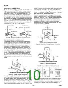
T he plot in Figure 4 was made using a slightly different tech-
nique. Here an FFT based instrument (Figure 31) is used to
generate a 10 Hz “brickwall” filter. A low frequency pole at
0.1 Hz is generated with an external ac coupling capacitor, the
instrument being dc coupled.
At very low source resistance (rS <50 Ω), the amplifiers’ voltage
noise dominates. As source resistance increases the Johnson
noise of rS dominates until at higher resistances (rS >2 kΩ) the
current noise component is larger than the resistor noise.
Several precautions are necessary to get optimum low frequency
noise performance:
1. Care must be used to account for the effects of rS, even a
10 Ω resistor has 0.4 nV/√Hz of noise (an error of 9% when
root sum squared with 0.9 nV/√Hz).
100
2. T he test set up must be fully warmed up to prevent eOS drift
from erroneously contributing to input noise.
3. Circuitry must be shielded from air currents. Heat flow out
of the package through its leads creates the opportunity for a
thermoelectric potential at every junction of different metals.
Selective heating and cooling of these by random air currents
will appear as 1/f noise and obscure the true device noise.
TOTAL NOISE
10
RESISTOR
NOISE
ONLY
1
4. T he results must be interpreted using valid statistical
techniques.
100kΩ
0.1
+VS
10
100
1000
10000
**
SOURCE RESISTANCE – Ω
1Ω
Figure 30. Noise vs. Source Resistance
2
3
7
HP 3465
1.5µF
DYNAMIC SIGNAL
ANALYZER
(10Hz)
T he AD797 is the optimum choice for low noise performance
provided the source resistance is kept <1 kΩ. At higher values of
source resistance, optimum performance with respect to noise
alone is obtained with other amplifiers from Analog Devices (see
T able I).
6
AD797
VOUT
4
**
–VS
** USE POWER SUPPLY BYPASSING SHOWN IN FIGURE 32.
Figure 31. Test Setup for Measuring 0.1 Hz to 10 Hz Noise
Table I. Recom m ended Am plifiers for D ifferent Source
Im pedances
WID EBAND NO ISE
rS, ohm s
Recom m ended Am plifier
T he AD797, due to its single stage design, has the property that
its noise is flat over frequencies from less than 10 Hz to beyond
1 MHz. T his is not true of most dc precision amplifiers where
second stage noise contributes to input referred noise beyond
the audio frequency range. T he AD797 offers new levels of per-
formance in wideband imaging applications. In sampled data
systems, where aliasing of out of band noise into the signal band
is a problem, the AD797 will out perform all previously avail-
able IC op amps.
0 to <1 k
AD797
1 k to <10 k
10 k to <100 k
>100 k
AD707, AD743/AD745, OP27/OP37, OP07
AD705, AD743/AD745, OP07
AD548, AD549, AD645, AD711, AD743/
AD745
REV. C
–9–

 ETC [ ETC ]