AD797
R1
TO TEKTRONIX
7A26
1MΩ
20pF
OSCILLOSCOPE
PREAMP INPUT
SECTION
50pF
R2
226
Ω
4.26kΩ
2
3
8
(VIA LESS THAN 1FT
50 COAXIAL CABLE)
Ω
6
AD797
2
3
V
X 5
250Ω
A2
AD829
V
IN
ERROR
6
7
2x
HP2835
4
a.
2x
HP2835
0.47µF
0.47µF
R1
+V
S
C2
C1
–V
S
1k
1k
Ω
Ω
R2
NOTE:
USE CIRCUIT
BOARD
WITH GROUND
PLANE
Ω
100
Ω
1k
2
3
8
TEKTRONIX
CALIBRATION
FIXTURE
6
AD797
V
IN
20pF
6
V
IN
1kΩ
2
3
C1, SEE TABLE
C2 = 50pF – C1
A1
AD797
51pF
7
b.
4
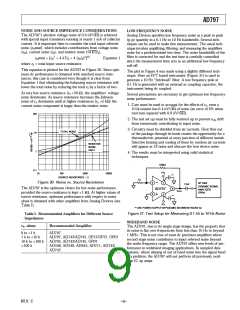
Figure 41. Recom m ended Connections for Distortion
Cancellation and Bandwidth Enhancem ent
0.1µF
1µF
0.1µF
–V
1µF
+V
S
S
Table IV. Recom m ended External Com pensation
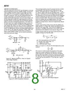
Figure 40. Settling Tim e Test Circuit
D ISTO RTIO N RED UCTIO N
The AD797 has distortion performance (T H D < –120 dB, @
20 kH z, 3 V rms, RL = 600 Ω) unequaled by most voltage
feedback amplifiers.
A/B
R1 R2 C1 C2 3 dB
(pF) BW
A
B
C1 C2 3 dB
(pF) BW
Ω
Ω
G = 10
909 100
G = 100 1 k 10
G = 1000 10 k 10
0
0
0
50 6 MHz
50 1 MHz
50 110 kHz 33 15 450 kHz
0
50 6 MHz
15 33 1.5 MHz
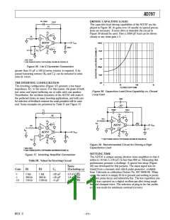
At higher gains and higher frequencies T HD will increase due
to reduction in loop gain. However in contrast to most conven-
tional voltage feedback amplifiers the AD797 provides two effec-
tive means of reducing distortion, as gain and frequency are
increased; cancellation of the output stage’s distortion and gain
bandwidth enhancement by decompensation. By applying these
techniques gain bandwidth can be increased to 450 MH z at
G = 1000 and distortion can be held to –100 dB at 20 kHz for
G = 100.
0.01
–80
–90
G=1000
R =600Ω
L
0.003
NOISE LIMIT, G=1000
NOISE LIMIT, G=100
G=1000
R =10kΩ
L
0.001
–100
–110
–120
G=100
R =600Ω
T he unique design of the AD797 provides for cancellation of the
output stage’s distortion (patent pending). T o achieve this a ca-
pacitance equal to the effective compensation capacitance, usu-
ally 50 pF, is connected between Pin 8 and the output (C2 in
Figure 41). Use of this feature will improve distortion perfor-
mance when the closed loop gain is more than 10 or when fre-
quencies of interest are greater than 30 kHz.
L
0.0003
0.0001
G=10
R =600Ω
L
100
300
1k
3k
10k
30k
100k
300k
Bandwidth enhancement via decompensation is achieved by
connecting a capacitor from Pin 8 to ground (C1 in Figure 41)
effectively subtracting from the value of the internal compensa-
tion capacitance (50 pF), yielding a smaller effective compensa-
tion capacitance and, therefore, a larger bandwidth. T he
benefits of this begin at closed loop gains of 100 and up. A
maximum value of ≈33 pF at gains of 1000 and up is recom-
mended. At a gain of 1000 the bandwidth is 450 kHz.
FREQUENCY – Hz
Figure 42. Total Harm onic Distortion (THD) vs. Frequency
@ 3 V rm s for Figure 41b
T able IV and Figure 42 summarize the performance of the
AD797 with distortion cancellation and decompensation.
–12–
REV. C

 ETC [ ETC ]