AD797
D iffer ential Line Receiver
A Gener al P ur pose ATE/Instr um entation Input/O utput
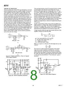
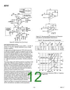
T he differential receiver circuit of Figure 43 is useful for many
applications from audio to MRI imaging. It allows extraction of
a low level signal in the presence of common-mode noise. As
shown in Figure 44, the AD797 provides this function with only
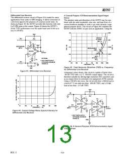
9 nV/√Hz noise at the output. Figure 45 shows the AD797’s
20-bit T HD performance over the audio band and 16-bit accu-
racy to 250 kHz.
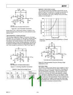
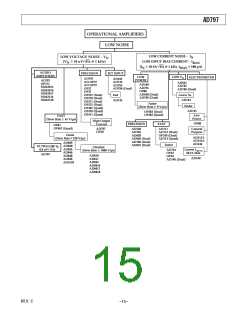
D r iver
T he ultralow noise and distortion of the AD797 may be com-
bined with the wide bandwidth, slew rate, and load drive of a
current feedback amplifier to yield a very wide dynamic range
general purpose driver. T he circuit of Figure 46 combines the
AD797 with the AD811 in just such an application. Using the
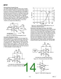
–90
–100
–110
–120
–130
0.003
20pF
WITHOUT
OPTIONAL
1kΩ
1kΩ
0.001
50pF C
N
+VS
**
50pF*
6
DIFFERENTIAL
INPUT
7
0.0003
0.0001
MEASUREMENT
LIMIT
2
3
8
AD797
OUTPUT
4
WITH
OPTIONAL
50C
*OPTIONAL
**
–VS
N
USE POWER SUPPLY
BYPASSING SHOWN IN
FIGURE 32.
**
1kΩ
1kΩ
100
300
1k
3k
10k
30k
100k
300k
FREQUENCY – Hz
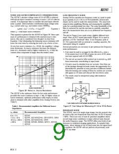
Figure 45. Total Harm onic Distortion (THD) vs. Frequency
for Differential Line Receiver
20pF
Figure 43. Differential Line Receiver
component values shown, this circuit is capable of better than
–90 dB T HD with a ±5 V, 500 kHz output signal. T he circuit is
therefore suitable for driving high resolution A/D converters and
as an output driver in automatic test equipment (AT E) systems.
Using a 100 kHz sine wave, the circuit will drive a 600 Ω load to
a level of 7 V rms with less than –109 dB T HD, and a 10 kΩ
load at less than –117 dB T HD.
16
14
12
10
8
22pF
R2
+V
S
2kΩ
**
+V
S
**
2
3
7
3
6
7
AD797
6
1kΩ
10
100
1k
10k
100k
1M
10M
4
6
AD811
FREQUENCY — Hz
**
INPUT
OUTPUT
2
4
**
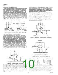
Figure 44. Output Voltage Noise Spectral Density for
Differential Line Receiver
–V
S
–V
649Ω
S
USE POWER SUPPLY
**
BYPASSING SHOWN IN
FIGURE 32.
649Ω
Figure 46. A General Purpose ATE/lnstrum entation Input/
Output Driver
REV. C
–13–

 ETC [ ETC ]