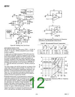
AD797
TH EO RY O F O P ERATIO N
T his matching benefits not just dc precision but since it holds
up dynamically, both distortion and settling time are also
reduced. T his single stage has a voltage gain of >5 × 10⁶ and
VOS <80 µV, while at the same time providing T HD + noise of
less than –120 dB and true 16 bit settling in less than 800 ns.
T he elimination of second stage noise effects has the additional
benefit of making the low noise of the AD797 (<0.9 nV/√Hz)
extend to beyond 1 MHz. T his means new levels of perfor-
mance for sampled data and imaging systems. All of this perfor-
mance as well as load drive in excess of 30 mA are made
possible by Analog Devices’ advanced Complementary Bipolar
(CB) process.
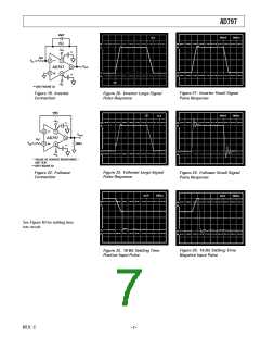
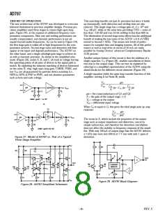
T he new architecture of the AD797 was developed to overcome
inherent limitations in previous amplifier designs. Previous pre-
cision amplifiers used three stages to ensure high open-loop
gain, Figure 27b, at the expense of additional frequency com-
pensation components. Slew rate and settling performance are
usually compromised, and dynamic performance is not ad-
equate beyond audio frequencies. As can be seen in Figure 27b,
the first stage gain is rolled off at high frequencies by the com-
pensation network. Second stage noise and distortion will then
appear at the input and degrade performance. T he AD797 on
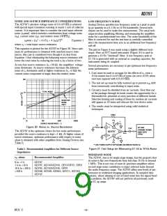
the other hand, uses a single ultrahigh gain stage to achieve dc
as well as dynamic precision. As shown in the simplified sche-
matic (Figure 28), nodes A, B, and C all track in voltage forcing
the operating points of all pairs of devices in the signal path to
match. By exploiting the inherent matching of devices fabricated
on the same IC chip, high open-loop gain, CMRR, PSRR, and
low VOS are all guaranteed by pairwise device matching (i.e.,
NPN to NPN & PNP to PNP), and not absolute parameters
such as beta and early voltage.
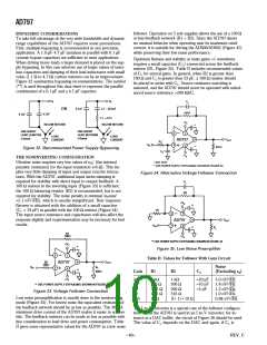
Another unique feature of this circuit is that the addition of a
single capacitor, CN (Figure 28), enables cancellation of distor-
tion due to the output stage. T his can best be explained by
referring to a simplified representation of the AD797 using ide-
alized blocks for the different circuit elements (Figure 29).
A single equation yields the open-loop transfer function of this
amplifier, solving it (at Node B) yields:
VO
VIN
gm
=
CN
A
CC
A
gm
BUFFER
V
OUT
jω –CN jω –
jω
R
R1
C1
L
gm = the transconductance of Q1 and Q2
A = the gain of the output stage, (~1)
VO = voltage at the output
6
GAIN = gmR1 5 x 10
VIN = differential input voltage
a.
When CN is equal to CC this gives the ideal single pole op amp
C2
A3
response:
VO
gm
=
VIN
jωC
gm
A2
C1
V
OUT
BUFFER
T he terms in A, which include the properties of the output
stage such as output impedance and distortion, cancel by
simple subtraction, and therefore the distortion cancellation
does not affect the stability or frequency response of the ampli-
fier. With only 500 µA of output stage bias the AD797 delivers
a 1 kHz sine wave into 600 Ω at 7 V rms with only 1 ppm of
distortion.
R1
R
L
R2
GAIN = gmR1 *A2 *A3
b.
Figure 27. Model of AD797 vs. That of a Typical
Three-Stage Am plifier
VCC
I1
I2
C
N
R2
R3
CN
R1
I5
Q4
B
A
OUT
Q10
Q11
Q3
Q7
A
A
B
OUT
–IN
+IN
C
C
Q9
CURRENT
MIRROR
Q2
I3
Q1
–IN
+IN
Q8
Q12
Q1 Q2
Q5
C
Q6
CC
1
I4
C
I6
I1
I7
I4
VSS
Figure 29. AD797 Block Diagram
Figure 28. AD797 Sim plified Schem atic
–8–
REV. C

 ETC [ ETC ]