AD797
11
10
9
140
120
100
+125°C
PSR
+SUPPLY
PSR
–SUPPLY
150
125
100
75
80
60
+25°C
–55°C
8
CMR
7
40
20
6
0
50
1M
5
15
20
10
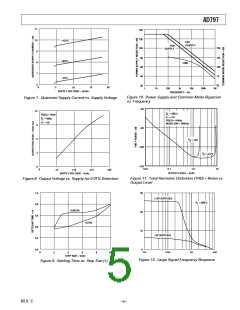
SUPPLY VOLTAGE – ±Volts
1
10
100
1k
10k
100k
FREQUENCY – Hz
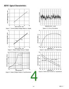
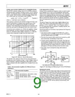
Figure 10. Power Supply and Com m on-Mode Rejection
vs. Frequency
Figure 7. Quiescent Supply Current vs. Supply Voltage
–60
12
R
= 600
Ω
L
FREQ = 1kHz
G = +10
FREQ = 10kHz
NOISE BW = 100kHz
R
= 600Ω
L
G = +10
9
6
3
0
–80
–100
–120
V
= ±5V
S
V
= ±15V
S
0.01
0.1
1.0
10
0
±5
±10
±15
±20
OUTPUT LEVEL – Volts
SUPPLY VOLTAGE – Volts
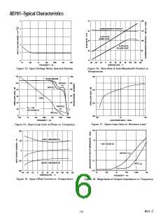
Figure 11. Total Harm onic Distortion (THD) + Noise vs.
Output Level
Figure 8. Output Voltage vs. Supply for 0.01% Distortion
30
1.0
0.8
±15V SUPPLIES
RL = 600Ω
0.0015%
20
0.6
0.01%
0.4
10
±5V SUPPLIES
0.2
0.0
0
0
2
4
6
8
10
STEP SIZE – Volts
Figure 12. Large Signal Frequency Response
Figure 9. Settling Tim e vs. Step Size (±)
REV. C
–5–

 ETC [ ETC ]