AD797
20–120pF
D RIVING CAP ACITIVE LO AD S
Ω
100
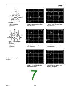
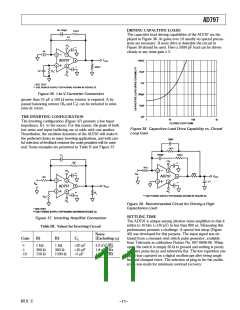
T he capacitive load driving capabilities of the AD797 are dis-
played in Figure 38. At gains over 10 usually no special precau-
tions are necessary. If more drive is desirable the circuit in
Figure 39 should be used. Here a 5000 pF load can be driven
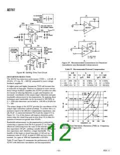
R1
+V
S
**
I
IN
cleanly at any noise gain
≥
2.
2
3
7
V
6
100nF
AD797
OUT
4
Ω
600
**
C
*
R
*
S
S
10nF
1nF
–V
S
* SEE TEXT
** USE POWER SUPPLY BYPASSING SHOWN IN FIGURE 32.
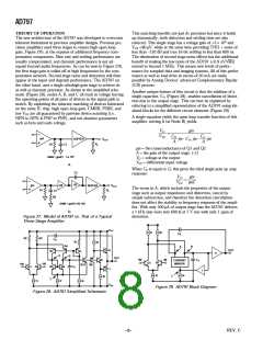
Figure 36. I-to-V Converter Connection
100pF
10pF
greater than 33 pF a 100 Ω series resistor is required. A by-
passed balancing resistor (RS and CS) can be included to mini-
mize dc errors.
1pF
1
TH E INVERTING CO NFIGURATIO N
10
100
1k
T he inverting configuration (Figure 37) presents a low input
impedance, R1, to the source. For this reason, the goals of both
low noise and input buffering are at odds with one another.
Nonetheless, the excellent dynamics of the AD797 will make it
the preferred choice in many inverting applications, and with care-
ful selection of feedback resistors the noise penalties will be mini-
mal. Some examples are presented in T able II and Figure 37.
CLOSED-LOOP GAIN
Figure 38. Capacitive Load Drive Capability vs. Closed
Loop Gain
20pF
Ω
1k
200pF
100
Ω
C
L
+V
S
R2
**
1k
Ω
2
+V
S
7
**
V
33Ω
IN
V
6
AD797
OUT
R1
2
7
C1
3
4
**
V
IN
6
V
OUT
AD797
–V
S
4
3
R
**
L
** USE POWER SUPPLY BYPASSING SHOWN IN FIGURE 32.
R
*
S
–V
S
Figure 39. Recom m ended Circuit for Driving a High
Capacitance Load
* SEE TEXT
** USE POWER SUPPLY BYPASSING SHOWN IN FIGURE 32.
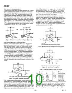
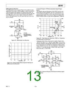
SETTLING TIME
Figure 37. Inverting Am plifier Connection
T he AD797 is unique among ultralow noise amplifiers in that it
settles to 16 bits (<150 µV) in less than 800 ns. Measuring this
performance presents a challenge. A special test setup (Figure
40) was developed for this purpose. T he input signal was ob-
tained from a resonant reed switch pulse generator, available
from T ektronix as calibration Fixture No. 067-0608-00. When
open, the switch is simply 50 Ω to ground and settling is purely
a passive pulse decay and inherently flat. T he low repetition rate
signal was captured on a digital oscilloscope after being ampli-
fied and clamped twice. T he selection of plug-in for the oscillo-
scope was made for minimum overload recovery.
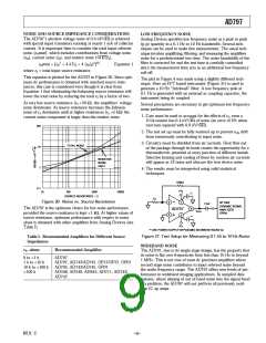
Table III. Values for Inverting Circuit
Noise
Gain
R1
R2
C L
(Excluding rS)
–1
–1
–10
1 kΩ
300 Ω
150 Ω
1 kΩ
300 Ω
1500 Ω
≈20 pF
≈10 pF
≈5 pF
3.0 nV/√Hz
1.8 nV/√Hz
1.8 nV/√Hz
REV. C
–11–

 ETC [ ETC ]