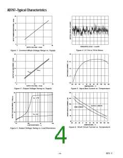
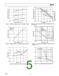
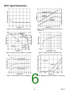
AD797
20pF
50mV
100ns
1µs
1kΩ
100
90
100
90
+V
S
**
1kΩ
V
2
3
7
IN
V
6
OUT
AD797
10
10
4
**
0%
0%
5V
–V
S
** SEE FIGURE 32
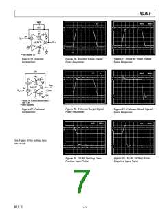
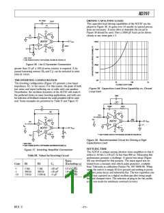
Figure 21. Inverter Sm all Signal
Pulse Response
Figure 19. Inverter
Connection
Figure 20. Inverter Large Signal
Pulse Response
100Ω
1µs
5V
50mV
100ns
+V
S
100
90
100
90
**
2
3
7
V
OUT
6
AD797
R *
S
V
600Ω
IN
4
**
10
10
0%
0%
–V
S
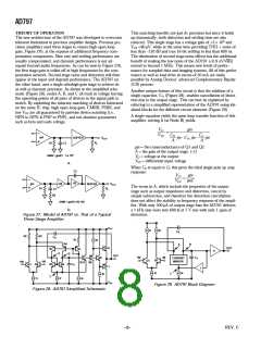
* VALUE OF SOURCE RESISTANCE –
SEE TEXT
** SEE FIGURE 32
Figure 23. Follower Large Signal
Pulse Response
Figure 22. Follower
Connection
Figure 24. Follower Sm all Signal
Pulse Response
5mV
500ns
5mV
500ns
100
90
100
90
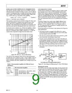
See Figure 40 for settling time
test circuit.
10
10
0%
0%
Figure 25. 16-Bit Settling Tim e
Positive Input Pulse
Figure 26. 16-Bit Settling Tim e
Negative Input Pulse
REV. C
–7–

 ETC [ ETC ]